Chapter 9 SDRAM Controller
9-11
9.3.4.2 Advanced
CKE
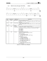
Advanced CKE is a function that speeds up the CKE assertion and deassertion timing by 1
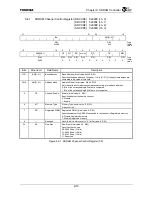
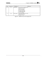
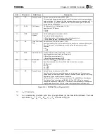
clock cycle. This function is set using the Address CKE bit (SDCTR.ACE) of the SDRAM Timing
Register.
Advanced CKE assumes that it will be used in a system where SDRAM data is saved even
when the power to the TX4925 itself is cut. Since CKE On/Off becomes 1 cycle faster, it is
possible to delay CKE by 1 clock cycle using external power consumption control logic. Please set
the SDRAM to the Self-Refresh mode before using this function.
When combining advanced CKE functionality with Power Down Auto Entry functionality and
memory access is requested while in the Power Down mode, two more SDCLK cycles of latency
are added than would be the case when not in the Power Down mode.
9.3.5 Bus
Errors
The SDRAMC detects bus errors in the following situations:
•
Bus time-out occurs during Read or Write operation to the SDRAMC
If a bus error occurs when accessing the SDRAMC, then the SDRAMC will immediately abort
current operation. Then, the current SDRAM cycle will end, remaining SDRAMC operations will be
aborted, a Pre-charge All command will be issued to SDRAM, then the SDRAMC will return to the Idle
state.
9.3.6
Memory Read and Memory Write
The RAS* signal, CAS* signal, WE*, signal, ADDR[19:16], SADDR10, and ADDR[14:5] signal are
set up 1 cycle before the SDCS* signal is asserted in the case of the Read command, Write command,
Pre-charge command, or Mode Register Set command. The same set up time is observed even for active
commands if the Active Command Ready bit (SDCTR.DA) of the SDRAM Timing Register is set.
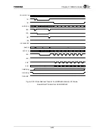
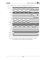
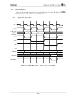
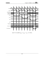
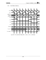
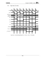
Figure 9.5.1 is a timing diagram of Single Read operation when the SDCTR.DA bit is cleared. Figure
9.5.2 is a timing diagram of Single Read operation when the SDCTR.DA bit is set.
Burst or Single Read operation is terminated by the Pre-charge Active Bank command. Burst or
Single Write operation is terminated by the Auto Pre-charge Command.
9.3.7 Slow
Write
Burst
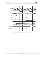
When the Slow Write Burst bit (SDCTR.SWB) of the SDRAM Timing Register is cleared, the data
changes at each cycle during Burst Write operation (Figure 9.5.6). When the Slow Write Burst bit is set,
the data will change every other cycle (Figure 9.5.7).
When Slow Write Burst bit is set, it always operates as t
RCD
= 3t
CK
against all write access in no
relation with the value of RAS-CAS Delay bit (SDCTR.RCD) of SDRAM Timing Register. When slow
write burst is invalid, the value of RAS-CAS Delay bit is valid. During read access the value of RAS-
CAS Delay bit is valid in no relation with Slow Write Burst bit setup.
Содержание TMPR4925
Страница 1: ...64 Bit TX System RISC TX49 Family TMPR4925 Rev 3 0 ...
Страница 4: ......
Страница 15: ...Handling Precautions ...
Страница 16: ......
Страница 18: ...1 Using Toshiba Semiconductors Safely 1 2 ...
Страница 40: ...3 General Safety Precautions and Usage Considerations 3 18 ...
Страница 42: ...4 Precautions and Usage Considerations 4 2 ...
Страница 43: ...TMPR4925 ...
Страница 44: ......
Страница 54: ...Chapter 1 Features 1 8 ...
Страница 58: ...Chapter 2 Block Diagram 2 4 ...
Страница 88: ...Chapter 4 Address Mapping 4 12 ...
Страница 226: ...Chapter 8 DMA Controller 8 58 ...
Страница 260: ...Chapter 9 SDRAM Controller 9 34 ...
Страница 480: ...Chapter 15 Interrupt Controller 15 32 ...
Страница 554: ...Chapter 19 Real Time Clock RTC 19 8 ...
Страница 555: ...Chapter 20 Removed 20 1 20 Removed ...
Страница 556: ...Chapter 20 Removed 20 2 ...
Страница 564: ...Chapter 21 Extended EJTAG Interface 21 8 ...
Страница 580: ...Chapter 22 Electrical Characteristics 22 16 ...
Страница 586: ...Chapter 23 Pin Layout Package 23 6 23 2 Package Package Type Package Code 256 pin PBGA PBGA 4L P BGA256 2727 1 27A4 ...
Страница 588: ...Chapter 24 Usage Notes 24 2 ...
Страница 590: ...Appendix A TX49 H2 Core Supplement A 2 ...

