Chapter 5 Configuration Register
5-9
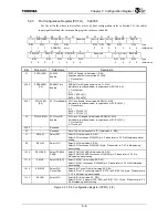
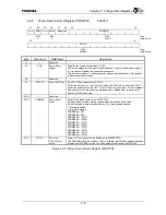
5.2.5
Power Down Control Register (PDNCTR)
0xE010
31 30 29 28 27 26 25
16
Reserved
PDN
Reserved
STPCPU
Reserved PDNMSK
R/W R/W
R/W
:
Type
0
0
0x3FF
: Initial value
15
0
PUTCV
R/W
:
Type
0x0000
: Initial value
Bits Mnemonic Field
Name
Description
31
⎯
Reserved
⎯
30 PDN
Power Down
Trigger
Power Down Trigger (Initial value: 0, R/W)
This bit is a trigger for the Power Down Sequence. It is set to 0 upon reset and a 0
to 1 transition will initiate the power down sequence.
This bit is not cleared to 0 automatically by wakeup from power down. Please clear
to 0 before next power down.
29
⎯
Reserved
⎯
28
STPCPU
Stop CPU Clock
Stop CPU Clock (Initial value: 0, R/W)
When this bit is set to 1, the CPU clock stops after TX49/H2 core operates WAIT
instruction and becomes the HALT mode. It is set to 0 upon reset. It is not cleared to
0 automatically by wakeup from power down mode. Please clear to 0 and set to 1
before next CPU clock stop.
27:26
⎯
Reserved
⎯
25:16 PDNMSK
Power Down
Mask
Power Down Mask (Initial value: 0x3FF, R/W)
Indicates which external interrupt signals wake from power down mode.
A bit is allocated to each interrupt source. Set 1 and enables wakeup.
1: Interrupt Enabled
0: Interrupt Disabled
PDNMSK[9] = RTC
PDNMSK[8] = NMI
PDNMSK[7] = INT[7]
PDNMSK[6] = INT[6]
PDNMSK[5] = INT[5]
PDNMSK[4] = INT[4]
PDNMSK[3] = INT[3]
PDNMSK[2] = INT[2]
PDNMSK[1] = INT[1]
PDNMSK[0] = INT[0]
15:0 PUTCV
Power Up
Time Counter
Value
Power Up Time Counter Value (Initial value: 0x0000, R/W)
This field determines the number of input clocks that expire after a wakeup has been
initiated from STANDBY mode. The clock signal of this counter is MSTRCLK.
Figure 5.2.5 Power Down Control Register (PDNCTR)
Содержание TMPR4925
Страница 1: ...64 Bit TX System RISC TX49 Family TMPR4925 Rev 3 0 ...
Страница 4: ......
Страница 15: ...Handling Precautions ...
Страница 16: ......
Страница 18: ...1 Using Toshiba Semiconductors Safely 1 2 ...
Страница 40: ...3 General Safety Precautions and Usage Considerations 3 18 ...
Страница 42: ...4 Precautions and Usage Considerations 4 2 ...
Страница 43: ...TMPR4925 ...
Страница 44: ......
Страница 54: ...Chapter 1 Features 1 8 ...
Страница 58: ...Chapter 2 Block Diagram 2 4 ...
Страница 88: ...Chapter 4 Address Mapping 4 12 ...
Страница 226: ...Chapter 8 DMA Controller 8 58 ...
Страница 260: ...Chapter 9 SDRAM Controller 9 34 ...
Страница 480: ...Chapter 15 Interrupt Controller 15 32 ...
Страница 554: ...Chapter 19 Real Time Clock RTC 19 8 ...
Страница 555: ...Chapter 20 Removed 20 1 20 Removed ...
Страница 556: ...Chapter 20 Removed 20 2 ...
Страница 564: ...Chapter 21 Extended EJTAG Interface 21 8 ...
Страница 580: ...Chapter 22 Electrical Characteristics 22 16 ...
Страница 586: ...Chapter 23 Pin Layout Package 23 6 23 2 Package Package Type Package Code 256 pin PBGA PBGA 4L P BGA256 2727 1 27A4 ...
Страница 588: ...Chapter 24 Usage Notes 24 2 ...
Страница 590: ...Appendix A TX49 H2 Core Supplement A 2 ...


