Chapter 16 CHI Module
16-16
16.3.8 Configurations
The programmability of the clock, sync, bit offsets, and number of timeslots allows the CHI Module
to support a wide range of configurations. Several of these configurations are commonly utilized as
communication interfaces by numerous commercial products, some of which are briefly discussed
below. Other configurations are available for application-specific usage.
The K2 Interface is an AT&T standard used as a serial inter-chip digital interface between U-interface
transmission circuits and various system-wide interface circuits. The K2 Interface utilizes four pins
(clock, sync, data in, and data out) and consists of eight 8-bit timeslots, with a frame rate of 8 kHz and a
clock rate of 512 kHz.
The SLD Interface utilizes 3 pins (clock, sync, data), with the transmit and receive pins tied together,
such that the data is sent bi-directionally in a ping-pong fashion. The SLD Interface consists of eight 8-
bit timeslots, with 4 timeslots reserved for transmit and 4 timeslots reserved for receive. The frame rate
is 8 kHz and the clock rate is 512 kHz.
The GCI Interface is a 4-pin variable-speed TDM highway utilizing anywhere from 4 to 48 timeslots.
The frame rate is 8 kHz and the clock rate is 2x the data rate and varies from 512-kHz to 6.144 MHz.
The IOM-2 Interface is commonly used to interface to 4-pin ISDN line interface drivers. Each frame
consists of twelve 8-bit timeslots, with a frame rate of 8 kHz and a (2x) clock rate of 1.536-MHz.
The CEPT Level-1 PCM Format is a common communications standard used for digital transmission
of voice and data. Each frame consists of 32 8-bit timeslots, with a frame rate of 8-kHz and a (1x) clock
rate of 2.048 MHz.
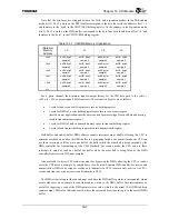
Table 16.3.4 shows a summary matrix of several example CHI configurations and their associated
parameters.
Table 16.3.4 Example CHI Configurations (Table Values Based on IMBUSCLKF
=
32.256 MHz)
CHICLK
Divide
Time Slots
CHICLK
Mode
fs CHICLK
Rate
Data
Rate Comments
4
64
2x
8 kHz
8.064 MHz
4.032 Mbps
slave mode only
6
48
2x
8 kHz
5.376 MHz
2.688 Mbps
GCI format
8
64
1x
8 kHz
4.032 MHz
4.032 Mbps
CHI format
8
8
1x
64 kHz
4.032 MHz
4.032 Mbps
hi-speed mode
9
64
1x
7.2 kHz
3.584 MHz
3.584 Mbps
11
24
2x
8 kHz
2.932 MHz
1.466 Mbps
11
48
1x
8 kHz
2.932 MHz
2.932 Mbps
16
32
1x
8 kHz
2.016 MHz
2.016 Mbps
CEPT PCM format
21
12
2x
8 kHz
1.536 MHz
768 kbps
IOM-2 format
63
8
1x
8 kHz
512 kHz
512 kbps
K2, SLD formats
Note that the maximum achievable frame rate depends on the system configuration. If devices with
long access time and/or 16 bit-wide data bus are used, the frame rate of 64 kHz may be unachievable
because of the reduced bus band width. Using other interfaces in parallel with CHI and/or reducing the
CPU clock frequencies will also reduce the band width available for CHI.
Содержание TMPR4925
Страница 1: ...64 Bit TX System RISC TX49 Family TMPR4925 Rev 3 0 ...
Страница 4: ......
Страница 15: ...Handling Precautions ...
Страница 16: ......
Страница 18: ...1 Using Toshiba Semiconductors Safely 1 2 ...
Страница 40: ...3 General Safety Precautions and Usage Considerations 3 18 ...
Страница 42: ...4 Precautions and Usage Considerations 4 2 ...
Страница 43: ...TMPR4925 ...
Страница 44: ......
Страница 54: ...Chapter 1 Features 1 8 ...
Страница 58: ...Chapter 2 Block Diagram 2 4 ...
Страница 88: ...Chapter 4 Address Mapping 4 12 ...
Страница 226: ...Chapter 8 DMA Controller 8 58 ...
Страница 260: ...Chapter 9 SDRAM Controller 9 34 ...
Страница 480: ...Chapter 15 Interrupt Controller 15 32 ...
Страница 554: ...Chapter 19 Real Time Clock RTC 19 8 ...
Страница 555: ...Chapter 20 Removed 20 1 20 Removed ...
Страница 556: ...Chapter 20 Removed 20 2 ...
Страница 564: ...Chapter 21 Extended EJTAG Interface 21 8 ...
Страница 580: ...Chapter 22 Electrical Characteristics 22 16 ...
Страница 586: ...Chapter 23 Pin Layout Package 23 6 23 2 Package Package Type Package Code 256 pin PBGA PBGA 4L P BGA256 2727 1 27A4 ...
Страница 588: ...Chapter 24 Usage Notes 24 2 ...
Страница 590: ...Appendix A TX49 H2 Core Supplement A 2 ...

