Chapter 11 Serial I/O Port
11-17
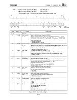
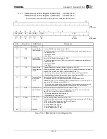
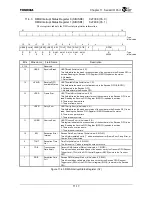
11.4.3 DMA/Interrupt Status Register 0 (SIDISR0)
0xF308 (Ch. 0)
DMA/Interrupt Status Register 1 (SIDISR1)
0xF408 (Ch. 1)
These registers indicate the DMA or interrupt status information.
31
16
0
:
Type
:
Initial
value
15 14 13 12 11 10 9 8 7 6 5 4
0
UBRK
UVALID
UFER UPER UOER ERI TOUT
TDIS RDIS
STIS
0
RFDN
R R R R R
R/W0C R/W0C R/W0C R/W0C R/W0C
R
:
Type
0 1 0 0 0 0 0 1 0 0
00000
:
Initial
value
Bits Mnemonic Field
Name
Description
31:16
⎯
Reserved
⎯
15
UBRK
Receive Break
UART Break (Initial value: 0, R)
This field indicates the break reception status of the next data in the Receive FIFO to
be read. Reading the Receive FIFO Register (SIRFIFO) updates the status.
0: No breaks
1: Detect breaks
14 UVALID
Receive FIFO
Available Status
UART Available Data (Initial value: 1, R)
This field indicates whether or not data exists in the Receive FIFO (SIRFIFO).
0: Data exists in the Receive FIFO.
1: No data exists in the Receive FIFO.
13
UFER
Frame Error
UART Frame Error (Initial value: 0, R)
This field indicates the frame error status of the next data in the Receive FIFO to be
read. Reading the Receive FIFO Register (SIRFIFO) updates the status.
0: There are no frame errors.
1: There are frame errors.
12
UPER
Parity Error
UART Parity Error (Initial value: 0, R)
This field indicates the parity error status of the next data in the Receive FIFO to be
read. Reading the Receive FIFO Register (SIRFIFO) updates the status.
0: There are no parity errors.
1: There are parity errors.
11
UOER
Overrun Error
UART Overrun Error (Initial value: 0, R)
This register indicates the overrun status of the next data in the Receive FIFO to be
read. Reading the Receive FIFO Register (SIRFIFO) updates the status.
0: There are no overrun errors.
1: There are overrun errors.
10 ERI
Reception Error
Interrupt
Receive Data Error Interrupt (Initial value: 0, R/W0C)
This bit is immediately set to “1” when a reception error (Frame Error, Parity Error, or
Overrun Error) is detected.
9 TOUT
Reception Time
Out
Time Out (Initial value: 0, R/W0C)
This bit is set to “1” when a reception time out occurs.
8 TDIS
Transmission
Data Empty
Transmit DMA/Interrupt Status (Initial value: 1, R/W0C)
This bit is set when available space of the amount set by the Transmit FIFO Request
Trigger Level (TDIL) of the FIFO Control Register (SIFCR) exists in the Transmit
FIFO.
7 RDIS
Reception Data
Full
Receive DMA/Interrupt Status (Initial value: 0, R/W0C)
This bit is set when valid data of the amount set by the Receive FIFO Request
Trigger Level (RDIL) of the FIFO Control register (SIFCR) is stored in the Receive
FIFO.
Figure 11.4.3 DMA/Interrupt Status Register (1/2)
Содержание TMPR4925
Страница 1: ...64 Bit TX System RISC TX49 Family TMPR4925 Rev 3 0 ...
Страница 4: ......
Страница 15: ...Handling Precautions ...
Страница 16: ......
Страница 18: ...1 Using Toshiba Semiconductors Safely 1 2 ...
Страница 40: ...3 General Safety Precautions and Usage Considerations 3 18 ...
Страница 42: ...4 Precautions and Usage Considerations 4 2 ...
Страница 43: ...TMPR4925 ...
Страница 44: ......
Страница 54: ...Chapter 1 Features 1 8 ...
Страница 58: ...Chapter 2 Block Diagram 2 4 ...
Страница 88: ...Chapter 4 Address Mapping 4 12 ...
Страница 226: ...Chapter 8 DMA Controller 8 58 ...
Страница 260: ...Chapter 9 SDRAM Controller 9 34 ...
Страница 480: ...Chapter 15 Interrupt Controller 15 32 ...
Страница 554: ...Chapter 19 Real Time Clock RTC 19 8 ...
Страница 555: ...Chapter 20 Removed 20 1 20 Removed ...
Страница 556: ...Chapter 20 Removed 20 2 ...
Страница 564: ...Chapter 21 Extended EJTAG Interface 21 8 ...
Страница 580: ...Chapter 22 Electrical Characteristics 22 16 ...
Страница 586: ...Chapter 23 Pin Layout Package 23 6 23 2 Package Package Type Package Code 256 pin PBGA PBGA 4L P BGA256 2727 1 27A4 ...
Страница 588: ...Chapter 24 Usage Notes 24 2 ...
Страница 590: ...Appendix A TX49 H2 Core Supplement A 2 ...


