Chapter 16 CHI Module
16-6
16.3.4 DMA
Address
Generation
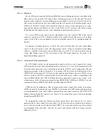
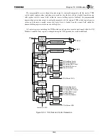
The CHI Module provides support for 2 full-duplex DMA channels: receive and transmit. The circuit
used to generate the DMA address, as well as half-buffer and end-of-buffer interrupts is shown in Figure
16.3.3.
Figure 16.3.3 CHI DMA Address Generation
The DMA buffer size is programmable (from a minimum of 16bytes up to a maximum of 16 Kbytes)
and the receive and transmit buffer start addresses are also programmable (anywhere over the full 32-bit
address space). Because there are separate start addresses, the receive and transmit buffers can be
configured to either reside in different memory spaces or share the same memory space. But in the
loopback mode, it can only share the same memory space and this ordering allows a receive-to-transmit
immediate via the DMA buffer. Thus, received samples are written to the DMA buffer location
immediately after transmit samples were read from that same location (which then became immediately
available). This ordering allows a single circular DMA buffer to be used for both transmit and receive
samples.
The DMA buffers can be configured in a circular buffer mode or a one-time buffer mode. For the
circular mode, the DMA address is continuously incremented (each time a DMA acknowledge is
received from the TX4925’s central DMA controller) and rolls over back to the start address after the
end-of-buffer is reached and will continue operating in a continuous and circular manner. For the one-
time mode, the DMA logic will stop executing whenever the end-of-buffer is reached.
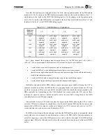
Because the CHI Module reads and writes a byte at a time between the shift registers and the 32 bit
holding registers, the software must pack and unpack these bytes to and from the 32 bit words in
memory in order to multiplex and demultiplex each channel for processing. Table 16.3.1 shows the
format and organization of the CHI channels within memory for DMA mode. Consecutive byte samples
for a given channel reside in memory every 8th byte.
12
30
12
12
Half-buffer
Interrupt
One-time VS.
Circular mode
End-of-buffer
Interrupt
DMA
Control from CPU
DMA ADDR
RX
Start
ADDR
DMA RD/WR mode
CLK
30
TX
Start
ADDR
2:1
DMA
CNTL
REG
CNT
Load
Logic
Buffer
Size
CMP
CMP
ADDR CNT
÷
2
Содержание TMPR4925
Страница 1: ...64 Bit TX System RISC TX49 Family TMPR4925 Rev 3 0 ...
Страница 4: ......
Страница 15: ...Handling Precautions ...
Страница 16: ......
Страница 18: ...1 Using Toshiba Semiconductors Safely 1 2 ...
Страница 40: ...3 General Safety Precautions and Usage Considerations 3 18 ...
Страница 42: ...4 Precautions and Usage Considerations 4 2 ...
Страница 43: ...TMPR4925 ...
Страница 44: ......
Страница 54: ...Chapter 1 Features 1 8 ...
Страница 58: ...Chapter 2 Block Diagram 2 4 ...
Страница 88: ...Chapter 4 Address Mapping 4 12 ...
Страница 226: ...Chapter 8 DMA Controller 8 58 ...
Страница 260: ...Chapter 9 SDRAM Controller 9 34 ...
Страница 480: ...Chapter 15 Interrupt Controller 15 32 ...
Страница 554: ...Chapter 19 Real Time Clock RTC 19 8 ...
Страница 555: ...Chapter 20 Removed 20 1 20 Removed ...
Страница 556: ...Chapter 20 Removed 20 2 ...
Страница 564: ...Chapter 21 Extended EJTAG Interface 21 8 ...
Страница 580: ...Chapter 22 Electrical Characteristics 22 16 ...
Страница 586: ...Chapter 23 Pin Layout Package 23 6 23 2 Package Package Type Package Code 256 pin PBGA PBGA 4L P BGA256 2727 1 27A4 ...
Страница 588: ...Chapter 24 Usage Notes 24 2 ...
Страница 590: ...Appendix A TX49 H2 Core Supplement A 2 ...


