Chapter 17 Serial Peripheral Interface
17-4
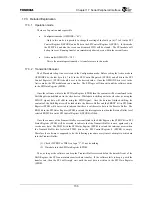
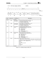
At the end of every series of transmission the software is supposed to negate the chip select signal for
the target device by the following procedure.
(1) Check if SRRDY or RBSI is a logic “1”. If not, do nothing.
(2) Check if SIDLE is a logic “1”. If not, do nothing.
(3) Negate the chip select signal.
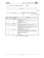
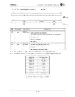
The SPI supports either 8-bit per character or 16-bit per character operation, as defined by the SSZ
bits in the SPI Control Register 1 (SPCR1). The software can also select whether the MSB or LSB
should shift first using the SBOS bit in the SPI Control Register 0 (SPCR0). Another set of SPHA and
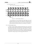
SPOL bits bit in the SPI Control Register 0 (SPCR0) select the transfer format. Please see to “17.3.4
Transfer Format”.
17.3.3 Baud Rate Generator
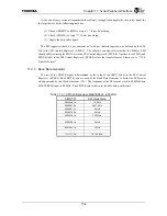
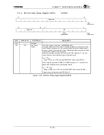
The rate of the SPICLK signal is determined by the value of the SER[7:0] bits in the SPI Control
Register 1 (SPCR1). The SER[7:0] bits are used by the Baud Rate Generator to devide the SPI master
clock generated by the Clock Generator (CG). The frequency of the SPI master clock is 40 MHz when
MASTERCLK input is 80 MHz. The SPICLK rate is shown in the table below in this time.
Table 17.3.1 SPICLK Rate when MASTERCLK is 80 MHz
SER[7:0]
SPI Clock Rate
00000001b 10
MHz
00000010b 6.667
MHz
00000011b 5
MHz
00000100b 4
MHz
00000101b 3.33
MHz
…
00001001b 2
MHz
…
00010011b 1
MHz
…
11111111b 78.125
KHz
Содержание TMPR4925
Страница 1: ...64 Bit TX System RISC TX49 Family TMPR4925 Rev 3 0 ...
Страница 4: ......
Страница 15: ...Handling Precautions ...
Страница 16: ......
Страница 18: ...1 Using Toshiba Semiconductors Safely 1 2 ...
Страница 40: ...3 General Safety Precautions and Usage Considerations 3 18 ...
Страница 42: ...4 Precautions and Usage Considerations 4 2 ...
Страница 43: ...TMPR4925 ...
Страница 44: ......
Страница 54: ...Chapter 1 Features 1 8 ...
Страница 58: ...Chapter 2 Block Diagram 2 4 ...
Страница 88: ...Chapter 4 Address Mapping 4 12 ...
Страница 226: ...Chapter 8 DMA Controller 8 58 ...
Страница 260: ...Chapter 9 SDRAM Controller 9 34 ...
Страница 480: ...Chapter 15 Interrupt Controller 15 32 ...
Страница 554: ...Chapter 19 Real Time Clock RTC 19 8 ...
Страница 555: ...Chapter 20 Removed 20 1 20 Removed ...
Страница 556: ...Chapter 20 Removed 20 2 ...
Страница 564: ...Chapter 21 Extended EJTAG Interface 21 8 ...
Страница 580: ...Chapter 22 Electrical Characteristics 22 16 ...
Страница 586: ...Chapter 23 Pin Layout Package 23 6 23 2 Package Package Type Package Code 256 pin PBGA PBGA 4L P BGA256 2727 1 27A4 ...
Страница 588: ...Chapter 24 Usage Notes 24 2 ...
Страница 590: ...Appendix A TX49 H2 Core Supplement A 2 ...


