Chapter 7 External Bus Controller
7-19
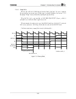
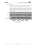
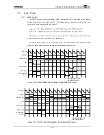
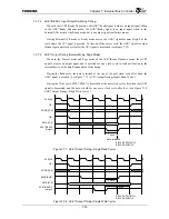
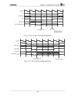
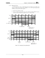
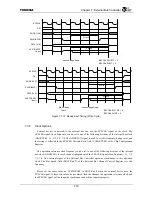
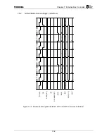
Figure 7.3.15 Ready Input Timing (Write Cycle)
7.3.8 Clock
Options
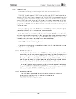
External devices connected to the external bus can use the SYSCLK signal as the clock. The
SYSCLK signal clock frequency can be set to one of the following divisions of the internal bus clock
(GBUSCLK): 1/1, 1/2, 1/3, 1/4. The ADDR[4:3] signal is used to set this frequency during reset, and
the setting is reflected in the SYSCLK Division Ratio field (CCFG.SYSSP) of the Chip Configuration
Register.
The operation reference clock frequency can be set to one of the following divisions of the internal
bus clock (GBUSCLK) for each channel independent of the SYSCLK signal clock frequency: 1/1, 1/2,
1/3, 1/4. The external signal of the External Bus Controller operates synchronous to this operation
clock. The Bus Speed field (EBCCRn.SP) of the External Bus Channel Control Register sets this
frequency.
Please set the same value as CCFG.SYSSP to EBCCRn.SP when the external device uses the
SYSCLK signal. If these two values do not match, then the channel, the operation reference clock, and
the SYSCLK signal will no longer be synchronous and will not operate properly.
3 clock
4 clock
SYSCLK
CE
*
ADDR [19:0]
SWE
*
/BWE
*
DATA [31:0]
ACK
*
/READY
(
Input
)
Acknowledge Read
EBCCRn.PWT:WT = 2
EBCCRn.SHWT = 0
Start Ready
Check
SYSCLK
CE
*
ADDR [19:0]
SWE
*
/BWE
*
DATA [31:0]
ACK
*
/READY
(Input)
3 clock
4 clock
Acknowledge Read
EBCCRn.PWT:WT = 2
EBCCRn.SHWT = 0
Содержание TMPR4925
Страница 1: ...64 Bit TX System RISC TX49 Family TMPR4925 Rev 3 0 ...
Страница 4: ......
Страница 15: ...Handling Precautions ...
Страница 16: ......
Страница 18: ...1 Using Toshiba Semiconductors Safely 1 2 ...
Страница 40: ...3 General Safety Precautions and Usage Considerations 3 18 ...
Страница 42: ...4 Precautions and Usage Considerations 4 2 ...
Страница 43: ...TMPR4925 ...
Страница 44: ......
Страница 54: ...Chapter 1 Features 1 8 ...
Страница 58: ...Chapter 2 Block Diagram 2 4 ...
Страница 88: ...Chapter 4 Address Mapping 4 12 ...
Страница 226: ...Chapter 8 DMA Controller 8 58 ...
Страница 260: ...Chapter 9 SDRAM Controller 9 34 ...
Страница 480: ...Chapter 15 Interrupt Controller 15 32 ...
Страница 554: ...Chapter 19 Real Time Clock RTC 19 8 ...
Страница 555: ...Chapter 20 Removed 20 1 20 Removed ...
Страница 556: ...Chapter 20 Removed 20 2 ...
Страница 564: ...Chapter 21 Extended EJTAG Interface 21 8 ...
Страница 580: ...Chapter 22 Electrical Characteristics 22 16 ...
Страница 586: ...Chapter 23 Pin Layout Package 23 6 23 2 Package Package Type Package Code 256 pin PBGA PBGA 4L P BGA256 2727 1 27A4 ...
Страница 588: ...Chapter 24 Usage Notes 24 2 ...
Страница 590: ...Appendix A TX49 H2 Core Supplement A 2 ...


