Chapter 10 PCI Controller
10-14
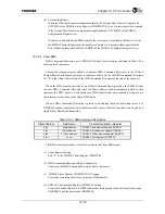
Initial state operation matches the correspondence between the address and byte data regardless of the
endian mode (operation is address consistent). For example, if WORD (16-bit) data is written to address
0 of the PCI Bus when the TX4925 is in the Big Endian mode, the upper byte (address 0 in Big Endian)
is written to PCI Bus address 0 and the lower byte (address 1 in Big Endian) is written to address 1 of
the PCI Bus. For Little Endian PCI devices, this means that the byte order is reversed.
When in the Big Endian mode and a particular access window Endian switching mechanism is
validated, data is transferred so the byte order does not change in DWORD (32-bit) access to that access
window.
Endian switching during initiator access is specified by the Byte Swap bit (BSWAPMn, BSWAPIO)
of the G2P Configuration Register (G2PCFG) of the access window for each initiator access (see Table
10.3.3).
Ending switching during target access is specified by the Byte Swap bit (BSWAP) of the G2P
Memory Space n Control Register (P2GMnCTR) or G2P I/O Space Control Register (P2GIOCTR) of
the access window for each target access.
10.3.8 Power
Management
The TX4925 PCI Controller supports power management functions that are compliant to PCI Bus
Power Management Interface Specifications Version 1.1 (Partially unsupported).
The PCI Host device controls the system status by reporting the power management state to the PCI
Satellite device.
10.3.8.1 Power Management State
In the case of the PCI Bus Power Management Interface Specifications, four power management
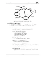
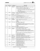
states are defined from State D0 to State D3. The TX4925 supports states D0 through D3. Figure 10.3.8
illustrates the power management state transition.
After Power On Reset, or when transitioning from the D3
HOT
state to the D0 state, the power
management state becomes uninitialized D0. If initialized by the system software at this point, the state
transitions to D0 Active.
If an external PCI Host device writes 11b (D3
HOT
) to the PowerState field of the Power Management
Control Status Register (PMCSR) of the Configuration space when in the Satellite mode, then the
Power Management State Change bit (P2GSTATUS.PMSC) of the P2G Status Register is set and
transitions to the D3
HOT
state. It then becomes possible to report Power State Change interrupts. The
PowerState field value can be read from the PowerState field (PCISSTATUS.PS) of the Satellite Mode
PCI Status Register.
The TX4925 uses software to change the system status after a status change is detected.
Содержание TMPR4925
Страница 1: ...64 Bit TX System RISC TX49 Family TMPR4925 Rev 3 0 ...
Страница 4: ......
Страница 15: ...Handling Precautions ...
Страница 16: ......
Страница 18: ...1 Using Toshiba Semiconductors Safely 1 2 ...
Страница 40: ...3 General Safety Precautions and Usage Considerations 3 18 ...
Страница 42: ...4 Precautions and Usage Considerations 4 2 ...
Страница 43: ...TMPR4925 ...
Страница 44: ......
Страница 54: ...Chapter 1 Features 1 8 ...
Страница 58: ...Chapter 2 Block Diagram 2 4 ...
Страница 88: ...Chapter 4 Address Mapping 4 12 ...
Страница 226: ...Chapter 8 DMA Controller 8 58 ...
Страница 260: ...Chapter 9 SDRAM Controller 9 34 ...
Страница 480: ...Chapter 15 Interrupt Controller 15 32 ...
Страница 554: ...Chapter 19 Real Time Clock RTC 19 8 ...
Страница 555: ...Chapter 20 Removed 20 1 20 Removed ...
Страница 556: ...Chapter 20 Removed 20 2 ...
Страница 564: ...Chapter 21 Extended EJTAG Interface 21 8 ...
Страница 580: ...Chapter 22 Electrical Characteristics 22 16 ...
Страница 586: ...Chapter 23 Pin Layout Package 23 6 23 2 Package Package Type Package Code 256 pin PBGA PBGA 4L P BGA256 2727 1 27A4 ...
Страница 588: ...Chapter 24 Usage Notes 24 2 ...
Страница 590: ...Appendix A TX49 H2 Core Supplement A 2 ...


