Chapter 3 Signals
3-10
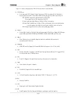
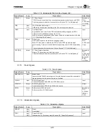
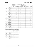
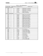
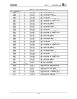
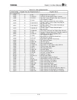
Table 3.1.14 Extended EJTAG Interface Signals (2/2)
Signal Name
Type
Description
Initial State
TPC[3:1] Output
PC
Trace
Output
TPC[3:1] output the value of the noncontiguous program counter in sync with DCLK.
The pins are shared with other functions (refer to Section "3.3 Pin Multiplexing").
Selected by
TDO
H: PIO input
L: All High
TMS Input
PU
JTAG Test Mode Select Input
TMS mainly controls state transition in the TAP controller state machine.
Input
TRST
*
Input
Test Reset Input
Asynchronous reset input for the TAP controller and debug support unit (DSU).
This pin must be pulled down to Low. (ex. 10 k
Ω
)
When this signal is deasserted, G-Bus timeout detection is disabled (refer to Section
“5.1.1 Detecting G-Bus Timeout”).
Input
DCLK Output
Debug
Clock
Clock output signal for the real-time debugging system.
When PC trace mode is selected, the TPC[3:1] and PCST signals are output
synchronously. This clock is the TX49/H2 core operating clock (CPUCLK) divided by
3.
The pin is shared with other functions (refer to Section "3.3 Pin Multiplexing").
Selected by
TDO
H: PIO input
L: Low
PCST[8:0]
Output
PC Trace Status Information
Outputs PC trace status and other information.
The pins are shared with other functions (refer to Section "3.3 Pin Multiplexing").
Selected by
TDO
H: PIO input
(PCST[8:1])
BC32K(PC
ST[0])
L: All Low
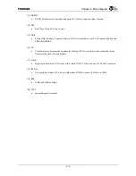
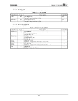
3.1.15 Clock
Signals
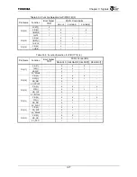
Table 3.1.15 Clock Signals
Signal Name
Type
Description
Initial State
MASTERCLK Input Master
Clock
Input pin for the TX4925 operating clock. A crystal resonator cannot be connected to
this pin because the pin does not contain an oscillator.
Input
C32KIN
Input
32 KHz Crystal Input
Connect this pin and C32KOUT to a 32.768 kHz crystal.
Input
C32KOUT
Output
32 KHz Crystal output
Connect this pin and C32KIN to a 32.768 kHz crystal.
Output
BC32K Output
PU
Buffer output of 32 KHz Crystal
Buffer output for a 32.768 kHz clock.
Selected by
TDO
H: Output
(BC32K)
L: Low
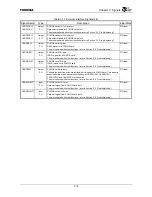
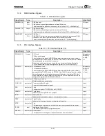
3.1.16 Initialization
Signals
Table 3.1.16 Initialization Signals
Signal Name
Type
Description
Initial State
RESET
*
Input
SMT
Reset
Reset signal.
Input
PON
*
Input
SMT
Power On Reset
Initializes the CG. For timing, refer to Section "6.3 Power-On Sequence".
Input
Содержание TMPR4925
Страница 1: ...64 Bit TX System RISC TX49 Family TMPR4925 Rev 3 0 ...
Страница 4: ......
Страница 15: ...Handling Precautions ...
Страница 16: ......
Страница 18: ...1 Using Toshiba Semiconductors Safely 1 2 ...
Страница 40: ...3 General Safety Precautions and Usage Considerations 3 18 ...
Страница 42: ...4 Precautions and Usage Considerations 4 2 ...
Страница 43: ...TMPR4925 ...
Страница 44: ......
Страница 54: ...Chapter 1 Features 1 8 ...
Страница 58: ...Chapter 2 Block Diagram 2 4 ...
Страница 88: ...Chapter 4 Address Mapping 4 12 ...
Страница 226: ...Chapter 8 DMA Controller 8 58 ...
Страница 260: ...Chapter 9 SDRAM Controller 9 34 ...
Страница 480: ...Chapter 15 Interrupt Controller 15 32 ...
Страница 554: ...Chapter 19 Real Time Clock RTC 19 8 ...
Страница 555: ...Chapter 20 Removed 20 1 20 Removed ...
Страница 556: ...Chapter 20 Removed 20 2 ...
Страница 564: ...Chapter 21 Extended EJTAG Interface 21 8 ...
Страница 580: ...Chapter 22 Electrical Characteristics 22 16 ...
Страница 586: ...Chapter 23 Pin Layout Package 23 6 23 2 Package Package Type Package Code 256 pin PBGA PBGA 4L P BGA256 2727 1 27A4 ...
Страница 588: ...Chapter 24 Usage Notes 24 2 ...
Страница 590: ...Appendix A TX49 H2 Core Supplement A 2 ...


