Chapter 21 Extended EJTAG Interface
21-3
21.2.2 Instruction
Register
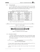
The JTAG Instruction Register consists of an 8-bit shift register. This register is used for selecting
either one or both of the test to be performed and the Test Data Register to be accessed. The Data
Register is selected according to the instruction code in Table 21.2.1. Refer to the “64-Bit TX System
RISC TX49/H2 Core Architecture” for more information regarding each instruction.
Table 21.2.1 Bit Configuration of JTAG Instruction Register
Instruction Code
MSB
→
LSB
Instruction Selected
Data
Register
00000000 (0x00)
EXTEST
Boundary Scan Register
00000001 (0x01)
SAMPLE/PRELOAD
Boundary Scan Register
00000010 (0x02)
Reserved
Reserved
00000011 (0x03)
IDCODE
Device ID Register
00000100 - 00001111
Reserved
Reserved
00010000 (0x10)
HIGHZ
Bypass Register
00010001 - 01111111
Reserved
Reserved
10000000 - 11111110
Refer to the TX49/H2 Core Architecture Manual
11111111 (0xFF)
BYPASS
Bypass Register
Figure 21.2.1 shows the format of the Instruction Register.
7 6 5 4 3 2 1 0
MSB
LSB
Figure 21.2.1 Instruction Register
The instruction code is shifted to the Instruction Register starting from the Least Significant Bit.
LSB
TDO
TDI
MSB
Figure 21.2.2 Shift Direction of the Instruction Register
21.2.3 Boundary Scan Register
The Boundary Scan Register contains a single 356-bit shift register to which all TX4925 I/O signals
except for power supply, TDI, TCK, TDO, TMS, TRST* are connected. TEST* and SCANENB*
cannot be tested, but it is possible for the Shift Register to sample the input. Figure 21.2.3 shows the
bits of the Boundary Scan Register.
355 0
Refer to TX4925 BSDL file.
Figure 21.2.3 Boundary Scan Register
TDI input is fetched to the Most Significant Bit (MSB) of the Boundary Scan Register and the Least
Significant Bit (LSB) of the Boundary Scan Register is sent from the TDO output.
Table 21.2.2 shows the boundary scan sequence relative to the processor signals. Control cells are omitted
in this table.
Содержание TMPR4925
Страница 1: ...64 Bit TX System RISC TX49 Family TMPR4925 Rev 3 0 ...
Страница 4: ......
Страница 15: ...Handling Precautions ...
Страница 16: ......
Страница 18: ...1 Using Toshiba Semiconductors Safely 1 2 ...
Страница 40: ...3 General Safety Precautions and Usage Considerations 3 18 ...
Страница 42: ...4 Precautions and Usage Considerations 4 2 ...
Страница 43: ...TMPR4925 ...
Страница 44: ......
Страница 54: ...Chapter 1 Features 1 8 ...
Страница 58: ...Chapter 2 Block Diagram 2 4 ...
Страница 88: ...Chapter 4 Address Mapping 4 12 ...
Страница 226: ...Chapter 8 DMA Controller 8 58 ...
Страница 260: ...Chapter 9 SDRAM Controller 9 34 ...
Страница 480: ...Chapter 15 Interrupt Controller 15 32 ...
Страница 554: ...Chapter 19 Real Time Clock RTC 19 8 ...
Страница 555: ...Chapter 20 Removed 20 1 20 Removed ...
Страница 556: ...Chapter 20 Removed 20 2 ...
Страница 564: ...Chapter 21 Extended EJTAG Interface 21 8 ...
Страница 580: ...Chapter 22 Electrical Characteristics 22 16 ...
Страница 586: ...Chapter 23 Pin Layout Package 23 6 23 2 Package Package Type Package Code 256 pin PBGA PBGA 4L P BGA256 2727 1 27A4 ...
Страница 588: ...Chapter 24 Usage Notes 24 2 ...
Страница 590: ...Appendix A TX49 H2 Core Supplement A 2 ...

