Chapter 8 DMA Controller
8-11
Example: When the transfer address is 0x0001_0000, the DMA Source Address Register
(DMSARn) is as follows below.
•
DMSAIRn setting is “0” or greater: 0x0001_0000
•
DMSAIRn setting is a negative value: 0x0001_0003
Table 8.3.3 Channel Register Setting Restrictions During Dual Address Transfer
DMSARn[1:0] DMDARn[1:0]
Transfer Setting
Size
(DMCCRn.XFSZ)
DMSAIRn
setting is 0
or greater
DMSAIRn
setting is a
negative
value
DMDAIRn
setting is 0
or greater
DMDAIRn
setting is a
negative
value
DMSAIRn DMDAIRn
DMCNTRn
[1:0]
DMCCRn.
REVBYTE
1 Byte
** **
**
**
** ** **
0
2 Bytes
*
0
*
1
*
0
*
1
*
0
*
0
*
0 0
4
Bytes
00 11 00 11 00 00 00 0/1
4 / 8 Wods
(DMMCR.FIFUM[n]
=
0)
00 11 00 11 00 00 00 0/1
00 11 00 11
4/0/-4
4/-4
‡
00 0/1
**
-
**
- 4 4
0
4 / 8 Words
(DMMCR.FIFUM[n]
=
1)
-
**
-
**
-4 -4
**
0
16 Words
Cannot be set (Configuration Error)
32 Words
Cannot be set (Configuration Error)
†: 4, 0 or -4 can be specified when Source Burst Inhibit bit (DMCCRn, SBINH) is set.
‡: 4, 0 or -4 can be specified when DestinationBurst Inhibit bit (DMCCRn.DBINH) is set.
8.3.8.2
Burst Transfer During Dual Address Transfer
The DMA Controller has a 32-bit 8-stage FIFO on-chip that is connected to the internal bus (G-
Bus) for Burst transfer during Dual Address transfer. Since this FIFO employs a shifter, it is
possible to perform transfer of any address or data size. Burst transfer is only performed when 4
Words or 8 Words is set by the Transfer Setting Size field (DMCCRn.XFSZ) and the FIFO Use
Enable bit (DMMCRn.FIFUM[n]) of the DMA Master Control Register is set.
According to the SDRAM Controller and External Bus Controller specifications, the DMA
Controller cannot perform Burst transfer that spans across 32 word boundaries. Consequently, if
the address that starts DMA transfer is not a multiple of the transfer setting size (DMCCRn.XFSZ)
(is not aligned), transfer cannot be performed by any of the transfer sizes that were specified by a
Burst transfer. Therefore, it is necessary to divide the transfer into multiple Burst transactions of a
transfer size smaller than the specified transfer size. This division method changes according to
the seting of the Transfer Size Mode bit (DMCCRn.USEXFSZ) of the DMA Channel Control
Register and whether or not the address offset relative to the Transfer Setting size
(DMCCRn.XFSZ) is equivalent to the source address and destination address combined.
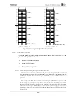
Figure 8.3.3 shows Dual Address Burst transfer when the Transfer Size Mode bit
(DMCCRn.USEXFSZ) is set to “1”, the lower 7 bits of the Transfer Start address for the transfer
source are set to 0x54, the lower 7 bits of the Transfer Start address for the transfer destination are
set to 0x1C, and the Transfer Setting Size (DMCCRn.XFSZ) is set to 8 Words.
Transfer repeats according to the transfer setting size, regardless of the different address offsets.
However, transfers that span across 32 word boundaries are divided. Since data remains in the on-
chip FIFO when in this mode, it becomes possible to share the on-chip FIFO among multiple
DMA channels.
Содержание TMPR4925
Страница 1: ...64 Bit TX System RISC TX49 Family TMPR4925 Rev 3 0 ...
Страница 4: ......
Страница 15: ...Handling Precautions ...
Страница 16: ......
Страница 18: ...1 Using Toshiba Semiconductors Safely 1 2 ...
Страница 40: ...3 General Safety Precautions and Usage Considerations 3 18 ...
Страница 42: ...4 Precautions and Usage Considerations 4 2 ...
Страница 43: ...TMPR4925 ...
Страница 44: ......
Страница 54: ...Chapter 1 Features 1 8 ...
Страница 58: ...Chapter 2 Block Diagram 2 4 ...
Страница 88: ...Chapter 4 Address Mapping 4 12 ...
Страница 226: ...Chapter 8 DMA Controller 8 58 ...
Страница 260: ...Chapter 9 SDRAM Controller 9 34 ...
Страница 480: ...Chapter 15 Interrupt Controller 15 32 ...
Страница 554: ...Chapter 19 Real Time Clock RTC 19 8 ...
Страница 555: ...Chapter 20 Removed 20 1 20 Removed ...
Страница 556: ...Chapter 20 Removed 20 2 ...
Страница 564: ...Chapter 21 Extended EJTAG Interface 21 8 ...
Страница 580: ...Chapter 22 Electrical Characteristics 22 16 ...
Страница 586: ...Chapter 23 Pin Layout Package 23 6 23 2 Package Package Type Package Code 256 pin PBGA PBGA 4L P BGA256 2727 1 27A4 ...
Страница 588: ...Chapter 24 Usage Notes 24 2 ...
Страница 590: ...Appendix A TX49 H2 Core Supplement A 2 ...

