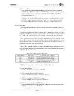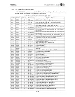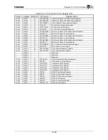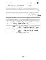
Chapter 10 PCI Controller
10-30
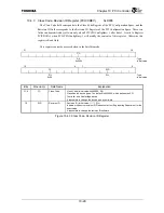
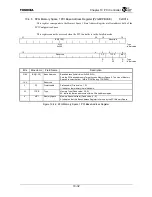
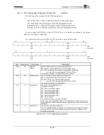
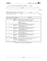
10.4.4 PCI Configuration 1 Register (PCICFG1)
0xD00C
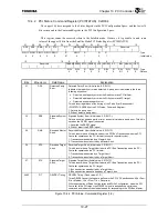
The following fields correspond to the following registers.
BIST
field
→
BIST Register of the PCI Configuration Space
Header Type field
→
Header Type Register in the PCI Configuration Space
Latency
Timer
field
→
Latency Timer Register of the PCI Configuration Space
Cache Line Size field
→
Cache Line Size Register of the PCI Configuration Space.
This register cannot be accessed when the PCI Controller is in the Satellite mode.
31
30
24
23
22
16
BISTC Reserved MFUNS
HT
R R
R/L
:
Type
0
0
0x00
: Initial value
15
8
7 0
LT CLS
R/W R/W
:
Type
0x00
0x00
: Initial value
Bits Mnemonic Field
Name
Description
31
BISTC
BIST Capable
BIST Capable (Fixed value: 0, R)
Indicates that the BIST function is not being supported.
30:24
⎯
Reserved
⎯
23
MFUNS
Multi-Function
Multi-Function (Fixed value: 0, R)
0: Indicates that the device is a single-function device.
22:16
HT
Header Type
Header Type (Initial value: 0x00, R/L)
Indicates the Header type.
0000000: Header Type 0
It is possible to change to the value that was written to the PCICDATA3 Register
when PCICCFG.LCFG is “1”.
15:8
LT
Latency Timer
Latency Timer (Initial value: 0x00, R/W)
Sets the latency timer value. Specifies the PCI Bus clock count during which to abort
access when the GNT
*
signal is deasserted during PCI access. Since the lower two
bits are fixed to “0”, cycle counts can only be specified in multiples of 4.
7:0
CLS
Cache Line Size
Cache Line Size (Initial value: 0x00, R/W)
Is used to select the PCI Bus command during a Burst Read transaction. See “10.3.3
Supported PCI Bus Commands)” for more information.
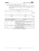
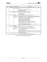
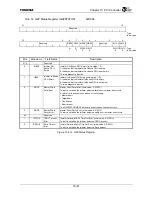
Figure 10.4.4 PCI Configuration 1 Register
Содержание TMPR4925
Страница 1: ...64 Bit TX System RISC TX49 Family TMPR4925 Rev 3 0 ...
Страница 4: ......
Страница 15: ...Handling Precautions ...
Страница 16: ......
Страница 18: ...1 Using Toshiba Semiconductors Safely 1 2 ...
Страница 40: ...3 General Safety Precautions and Usage Considerations 3 18 ...
Страница 42: ...4 Precautions and Usage Considerations 4 2 ...
Страница 43: ...TMPR4925 ...
Страница 44: ......
Страница 54: ...Chapter 1 Features 1 8 ...
Страница 58: ...Chapter 2 Block Diagram 2 4 ...
Страница 88: ...Chapter 4 Address Mapping 4 12 ...
Страница 226: ...Chapter 8 DMA Controller 8 58 ...
Страница 260: ...Chapter 9 SDRAM Controller 9 34 ...
Страница 480: ...Chapter 15 Interrupt Controller 15 32 ...
Страница 554: ...Chapter 19 Real Time Clock RTC 19 8 ...
Страница 555: ...Chapter 20 Removed 20 1 20 Removed ...
Страница 556: ...Chapter 20 Removed 20 2 ...
Страница 564: ...Chapter 21 Extended EJTAG Interface 21 8 ...
Страница 580: ...Chapter 22 Electrical Characteristics 22 16 ...
Страница 586: ...Chapter 23 Pin Layout Package 23 6 23 2 Package Package Type Package Code 256 pin PBGA PBGA 4L P BGA256 2727 1 27A4 ...
Страница 588: ...Chapter 24 Usage Notes 24 2 ...
Страница 590: ...Appendix A TX49 H2 Core Supplement A 2 ...

