Chapter 8 DMA Controller
8-16
8.3.10 Chain
DMA
Transfer
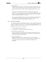
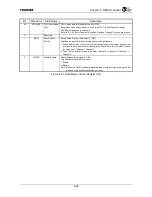
Table 8.3.4 shows the data structure in memory that the DMA Command Descriptor has. When the
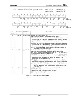
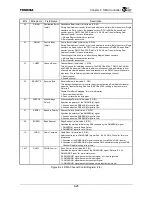
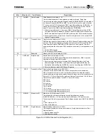
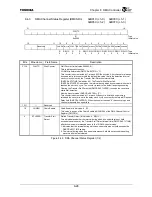
Simple Chain bit (SMPCHN) of the DMA Channel Control Register (DMCCRn) is set, only the initial
four words are used. DMSAIRn, DMDAIR, DMCCRn, and DMCSRn use the settings from when
DMA started. In addition, all eight words are used when the Simple Chain bit (SMPCHN) is cleared.
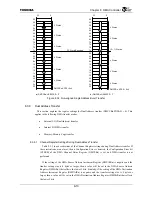
Saving the start memory address of another DMA Command Descriptor in the Offset 0 Chain
Address field makes it possible to construct a chain list of DMA Command Descriptors (Figure 8.3.5).
Set “0” in the Chain Address field of the DMA Command Descriptor at the end of the chain list.
When DMA transfer that is specified by one DMA Command Descriptor ends, the DMA Controller
automatically reads the next DMA Command Descriptor indicated by the Chain Address Register
(Chain transfer), then continues DMA transfer. Continuous DMA transfer that uses multiple Descriptors
connected into such a chain-like structure is called Chain DMA transfer.
Since the DMA Channel Status Register is also overwritten during Chain transfer when the DMA
Simple Chain bit (SMPCHN) is cleared, be sure not to unnecessarily clear necessary bits.
Placing DMA Command Descriptors at addresses that do not span across 32 word boundaries in
memory is efficient since they are read by one G-Bus Burst Read operation.
Table 8.3.4 DMA Command Descriptors
Offset Address
Field Name
Transfer Destination Register
0x00
Chain Address
DMA Chain Address Register (DMCHARn)
0x04
Source Address
DMA Source Address Register (DMSARn)
0x08
Destination Address
DMA Destination Address Register (DMDARn)
0x0c
Count
DMA Count Register (DMCNTRn)
0x10
Source Address Increment
DMA Source Address Increment Register (DMSAIRn)
0x14
Destination Address Increment
DMA Destination Address Increment Register (DMDAIRn)
0x18
Channel Control
DMA Channel Control Register (DMCCRn)
0x1c
Channel Status
DMA Channel Status Register (DMCSRn)
Figure 8.3.5 DMA Command Descriptor Chain
“A”
+
04
+
08
+
0c
+
10
+
14
+
18
+
1c
“B”
+
04
+
08
+
0c
+
10
+
14
+
18
+
1c
“C”
+
04
+
08
+
0c
+
10
+
14
+
18
+
1c
“D”
+
04
+
08
+
0c
+
10
+
14
+
18
+
1c
“E”
+
04
+
08
+
0c
+
10
+
14
+
18
+
1c
B
C
D
E
0
Содержание TMPR4925
Страница 1: ...64 Bit TX System RISC TX49 Family TMPR4925 Rev 3 0 ...
Страница 4: ......
Страница 15: ...Handling Precautions ...
Страница 16: ......
Страница 18: ...1 Using Toshiba Semiconductors Safely 1 2 ...
Страница 40: ...3 General Safety Precautions and Usage Considerations 3 18 ...
Страница 42: ...4 Precautions and Usage Considerations 4 2 ...
Страница 43: ...TMPR4925 ...
Страница 44: ......
Страница 54: ...Chapter 1 Features 1 8 ...
Страница 58: ...Chapter 2 Block Diagram 2 4 ...
Страница 88: ...Chapter 4 Address Mapping 4 12 ...
Страница 226: ...Chapter 8 DMA Controller 8 58 ...
Страница 260: ...Chapter 9 SDRAM Controller 9 34 ...
Страница 480: ...Chapter 15 Interrupt Controller 15 32 ...
Страница 554: ...Chapter 19 Real Time Clock RTC 19 8 ...
Страница 555: ...Chapter 20 Removed 20 1 20 Removed ...
Страница 556: ...Chapter 20 Removed 20 2 ...
Страница 564: ...Chapter 21 Extended EJTAG Interface 21 8 ...
Страница 580: ...Chapter 22 Electrical Characteristics 22 16 ...
Страница 586: ...Chapter 23 Pin Layout Package 23 6 23 2 Package Package Type Package Code 256 pin PBGA PBGA 4L P BGA256 2727 1 27A4 ...
Страница 588: ...Chapter 24 Usage Notes 24 2 ...
Страница 590: ...Appendix A TX49 H2 Core Supplement A 2 ...


