Chapter 10 PCI Controller
10-28
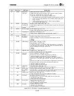
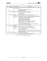
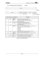
Bits Mnemonic Field
Name
Explanation
24 MDPE
Master Data
Parity Error
Master Data Parity Error (Initial value: 0, R/W1C)
Indicates the a parity error occurred when the PCI Controller is the PCI initiator.
This bit is not set when the PCI Controller is the target.
This bit is set when all of the three following conditions are met.
•
It has been detected that the PERR
*
signal was set either directly or indirectly.
•
The PCI Controller is the Bus Master for a PCI Bus transaction during which
an error occurred.
•
The Parity Error Response bit of the PCI Status Command Register
(PCISTATUS.PEREN) has been set.
23 FBBCP
Fast Back-to-
Back Capable
Fast Back-to-Back Capable (Fixed value: 1, R)
Indicates whether target access of a fast back-to-back transaction can be accepted.
Is fixed to “1”.
22
⎯
Reserved
⎯
21
66MCP
66 MHz Capable
66 MHz Capable (Fixed value: 0, R)
Indicates the 66 MHz operation is impossible. Is fixed to “0”.
20
CL
Capabilities List
Capabilities List (Fixed value: 1, R)
Indicates that the capabilities list is being implemented. Is fixed to “1”.
19:10
⎯
Reserved
⎯
9 FBBEN
Fast Back-to-
Back Enable
Fast Back-to-Back Enable (Initial value: 0, R/W)
Indicates that issuing of fast back-to-back transactions has been enabled.
1: Enable
0: Disable
8 SEREN
SERR
*
Enable
SERR
*
Enable (Initial value: 0, R/W)
Enables/Disables the SERR
*
signal.
The SERR
*
signal reports that either a PCI Bus address parity error or a special
cycle data parity error was detected. The SERR
*
signal is only asserted when the
Parity Error Response bit is set and this bit is set.
1: Enable
0: Disable
7
STPC
Stepping Control
Stepping Control (Fixed value: 0, R)
Indicates that stepping control is not being supported.
6 PEREN
Parity Error
Response
Parity Error Response (Initial value: 0, R/W)
Sets operation when a PCI address/data parity error is detected.
A parity error response (either when the Parity Error Response bit
(PCISTATUS.PEREN) of the PERR
*
Signal Assert or PCI Status, Command
Register is set, or the SERR
*
signal is asserted) is performed only when this bit is
set.
When this bit is cleared, the PCI Controller ignores all parity errors and continues
the transaction process as if the parity of that transaction was correct.
1: Parity error response is performed.
0: Parity error response is not performed.
5 VPS
VGA Palette
Snoop
VGA Palette Snoop (Fixed value: 0, R)
Indicates that the VGA palette snoop function is not supported.
4 MWIEN
Memory Write
and Invalidate
Enable
Memory Write and Invalidate Enable (Initial value: 0, R/W)
Controls whether to use the Memory Write and Invalidate command instead of the
Memory Write command when the PCI Controller is the initiator.
3
SC
Special Cycles
Special Cycles (Fixed value: 0, R)
Indicates that special cycles will not be accepted as PCI targets.
2 BM
Bus
Master
Bus Master (Initial value: 0/1, R/W)
The default is only “1” when in the PCI Boot mode and in the Host mode.
1: Operates as the Bus Master.
0: Does not operate as the Bus Master.
1 MEMSP
Memory
Space
Memory Space (Initial value: 0, R/W)
1: Respond to PCI memory access.
0: Do not respond to PCI memory access.
0 IOSP
I/O
Space
I/O Space (Initial value: 0, R/W)
1: Respond to PCI I/O access.
0: Do not respond to PCI I/O access.
Figure 10.4.2 PCI Status, Command Register (2/2)
Содержание TMPR4925
Страница 1: ...64 Bit TX System RISC TX49 Family TMPR4925 Rev 3 0 ...
Страница 4: ......
Страница 15: ...Handling Precautions ...
Страница 16: ......
Страница 18: ...1 Using Toshiba Semiconductors Safely 1 2 ...
Страница 40: ...3 General Safety Precautions and Usage Considerations 3 18 ...
Страница 42: ...4 Precautions and Usage Considerations 4 2 ...
Страница 43: ...TMPR4925 ...
Страница 44: ......
Страница 54: ...Chapter 1 Features 1 8 ...
Страница 58: ...Chapter 2 Block Diagram 2 4 ...
Страница 88: ...Chapter 4 Address Mapping 4 12 ...
Страница 226: ...Chapter 8 DMA Controller 8 58 ...
Страница 260: ...Chapter 9 SDRAM Controller 9 34 ...
Страница 480: ...Chapter 15 Interrupt Controller 15 32 ...
Страница 554: ...Chapter 19 Real Time Clock RTC 19 8 ...
Страница 555: ...Chapter 20 Removed 20 1 20 Removed ...
Страница 556: ...Chapter 20 Removed 20 2 ...
Страница 564: ...Chapter 21 Extended EJTAG Interface 21 8 ...
Страница 580: ...Chapter 22 Electrical Characteristics 22 16 ...
Страница 586: ...Chapter 23 Pin Layout Package 23 6 23 2 Package Package Type Package Code 256 pin PBGA PBGA 4L P BGA256 2727 1 27A4 ...
Страница 588: ...Chapter 24 Usage Notes 24 2 ...
Страница 590: ...Appendix A TX49 H2 Core Supplement A 2 ...


