Chapter 11 Serial I/O Port
11-8
11.3.6 DMA
Transfer
The DMA Request Control Register (DRQCTR)of the DMA Request Select field (DMAREQ[3:0])
can be used to allocate DMA channels for each reception and transmission channel in the following
manner.
SIO Channel 1 Reception
DMA Channel 0
SIO Channel 1 Transmission
DMA Channel 1
SIO Channel 0 Reception
DMA Channel 2
SIO Channel 0 Transmission
DMA Channel 3
Set the DMA Channel Control Register of the DMA Controller as described below.
DMA Request Polarity
Low Active
DMCCRn.ACKPOL = 0
DMA Acknowledge Polarity
Low Active
DMCCRn.REQPOL = 0
Request Detection
Level Detection
DMCCRn.EGREQ = 0
Transfer Size
1 Byte
DMCCRn.XFSZ = 000b
Transfer Address Mode
Dual
DMCCRn.SNGAD = 0
In the case of transmission channels, the address of the Transmit FIFO Register (SITFIFOn) is set in
the DMAC Destination Address Register (DMDARn). In the case of reception channels, the address of
the Receive FIFO Register (SIRFIFOn) is set in the DMAC Source Address Register (DMSARn).
Please set the addresses specified in “11.4.8 Transmit FIFO Register” and “11.4.9 Receive FIFO
Register” since the set address differs depending on the Endian mode.
11.3.7 Flow
Control
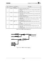
SIO supports hardware flow control that uses the RTS*/CTS* signal.
The CTS* (Clear to Send) input signal indicates that data can be received from the reception side
when it is Low. Setting the Transmission Enable Select bit (TES) of the Flow Control Register
(SIFLCRn) makes transmission flow control that uses the CTS* signal more effective.
It is also possible to generate status change interrupts by changing the state of the CTS* signal. The
conditions in which interrupts are generated can be selected by the CTSS Active Condition field of the
DMA/Interrupt Control Register (SIDICRn).
Setting the RTS* (Request to Send) output signal to High requests the transmission side to pause
transmission. Transmission resumes when the reception side becomes ready and the RTS* signal is set
to Low.
Setting the Reception Enable Select bit (RCS) of the flow Control Register (SIFLCRn) makes
reception flow control that uses the RTS* signal more effective. The RTS* signal pin status becomes
High when data of the byte count set by the RTS Active Trigger Level field (RTSTL) of the Flow
Control Register (SIFLCRn) accumulates in the Receive FIFO. The RTS* signal can also be made High
by setting the RTS Software Control bit (RTSSC) of the Flow Control Register (SIFLCRn). Setting this
bit requests the transmission side to pause transmission.
Содержание TMPR4925
Страница 1: ...64 Bit TX System RISC TX49 Family TMPR4925 Rev 3 0 ...
Страница 4: ......
Страница 15: ...Handling Precautions ...
Страница 16: ......
Страница 18: ...1 Using Toshiba Semiconductors Safely 1 2 ...
Страница 40: ...3 General Safety Precautions and Usage Considerations 3 18 ...
Страница 42: ...4 Precautions and Usage Considerations 4 2 ...
Страница 43: ...TMPR4925 ...
Страница 44: ......
Страница 54: ...Chapter 1 Features 1 8 ...
Страница 58: ...Chapter 2 Block Diagram 2 4 ...
Страница 88: ...Chapter 4 Address Mapping 4 12 ...
Страница 226: ...Chapter 8 DMA Controller 8 58 ...
Страница 260: ...Chapter 9 SDRAM Controller 9 34 ...
Страница 480: ...Chapter 15 Interrupt Controller 15 32 ...
Страница 554: ...Chapter 19 Real Time Clock RTC 19 8 ...
Страница 555: ...Chapter 20 Removed 20 1 20 Removed ...
Страница 556: ...Chapter 20 Removed 20 2 ...
Страница 564: ...Chapter 21 Extended EJTAG Interface 21 8 ...
Страница 580: ...Chapter 22 Electrical Characteristics 22 16 ...
Страница 586: ...Chapter 23 Pin Layout Package 23 6 23 2 Package Package Type Package Code 256 pin PBGA PBGA 4L P BGA256 2727 1 27A4 ...
Страница 588: ...Chapter 24 Usage Notes 24 2 ...
Страница 590: ...Appendix A TX49 H2 Core Supplement A 2 ...


