Chapter 7 External Bus Controller
7-21
7.3.9.3
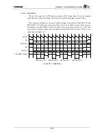
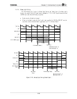
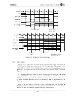
PCMCIA Channel Programming Requirements
Because of the multiple modes possible on a given EBUSC Channel the following restrictions
apply when a channel is used for PCMCIA access.
Page Mode is not allowed on a PCMCIA enabled Channel. Undetermined results will occur if
Page Mode is active.
External Ack Mode is not allowed on a PCMCIA enabled Channel. Undetermined results will
occur if External Ack Mode is active.
A channel that is used for PCMCIA access must be programmed to have a bus size of 16 or 8
bits. Addressing will not be correct if using a 32 bit bus size.
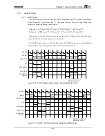
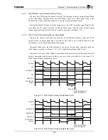
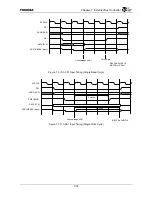
To meet the setup and hold timing of the PCMCIA bus the SHWT mode must be used.
Depending on the access speed of the card, the number of SHWT states and the speed of the
channel will need to be programmed to meet the timing requirements.
PWT and WT can be used to extend the OE*, WE*, CARDIORD*, and CARDIOWR* active
timing. See the description of the PWT and WT fields for details.
The EBUSC Controller can be used to implement the WAIT* function of the PCMCIA
specification. To do so PCMCIA channel must be programmed with the RDY bit set. See RDY
mode description for more details. Wait states will then be inserted externally until the WAIT*
signal from the PC card goes inactive and informing the EBUSC controller that it is READY. The
EBUSC controller supports a unique WAIT* signal for both slots. See device pin multiplexing for
details on support. The PWT/WT counter must be used programmed to account for the delay in
WAIT* valid from OE*, WE*, CARDIORD*, CARDIOWR*. Otherwise the high time of WAIT*
during this delay may cause the EBUSC controller to terminate the cycle early. The delay value
should take into account that the WAIT* signals are synchronized to the full speed clock
regardless of the speed of the channel.
7.3.9.4 PCMCIA
Addressing
and
UAE
The PCMCIA specification has a 26 bit address bus. Since the external address bus of the
device is only 20 bits, the top 6 bits must be latched using the UAE signal. See the description on
UAE for more details.
The PCMCIA specification always uses a byte addressing scheme, where A0 is a “don’t care”
for “Word” and “Odd-Byte-Only” accesses. Normally the EBUSC controller outputs an address
that allows for addressing bytes, half words, or words depending on the programmed bus size. For
accessing data sizes smaller than the programmed bus size the BE*/BWE* signals are used in
normal operations. In the case of a channel being used for PCMCIA access the addressing will
always be for bytes, regardless of the bus size being 16 or 8 bit.
7.3.9.5 PCMCIA
IOIS16
*
Signal
The IOIS16* signal is not supported. This means that the size of IO accesses needs to be known
ahead of time and are not dynamically sized.
Содержание TMPR4925
Страница 1: ...64 Bit TX System RISC TX49 Family TMPR4925 Rev 3 0 ...
Страница 4: ......
Страница 15: ...Handling Precautions ...
Страница 16: ......
Страница 18: ...1 Using Toshiba Semiconductors Safely 1 2 ...
Страница 40: ...3 General Safety Precautions and Usage Considerations 3 18 ...
Страница 42: ...4 Precautions and Usage Considerations 4 2 ...
Страница 43: ...TMPR4925 ...
Страница 44: ......
Страница 54: ...Chapter 1 Features 1 8 ...
Страница 58: ...Chapter 2 Block Diagram 2 4 ...
Страница 88: ...Chapter 4 Address Mapping 4 12 ...
Страница 226: ...Chapter 8 DMA Controller 8 58 ...
Страница 260: ...Chapter 9 SDRAM Controller 9 34 ...
Страница 480: ...Chapter 15 Interrupt Controller 15 32 ...
Страница 554: ...Chapter 19 Real Time Clock RTC 19 8 ...
Страница 555: ...Chapter 20 Removed 20 1 20 Removed ...
Страница 556: ...Chapter 20 Removed 20 2 ...
Страница 564: ...Chapter 21 Extended EJTAG Interface 21 8 ...
Страница 580: ...Chapter 22 Electrical Characteristics 22 16 ...
Страница 586: ...Chapter 23 Pin Layout Package 23 6 23 2 Package Package Type Package Code 256 pin PBGA PBGA 4L P BGA256 2727 1 27A4 ...
Страница 588: ...Chapter 24 Usage Notes 24 2 ...
Страница 590: ...Appendix A TX49 H2 Core Supplement A 2 ...

