Chapter 4 Address Mapping
4-2
4.2 Register
Map
4.2.1 Addressing
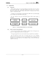
TX4925 internal registers are to be accessed through 64 K bytes address space that is based on
physical address 0xFF1F_0000 or pointed address by RAMP register (refer to 5.2.11). Figure 4.2.1
shows how to generate internal register address. Physical address 1 and physical address 2 shown
Figure 4.2.1 access the same register.
In TX49/H2 Core, the physical address form 0xFF00_0000 to 0xFF3F_FFFF are unchached mapped
to the virtual address form 0xFF00_0000 to 0xFF3F_FFFF.
This space includes the region form 0xFF1F_0000 allocated TX4925 internal registers at
initialization.
Figure 4.2.1 Generating Physical Address for a Internal Register
4.2.2
Ways to Access to Internal Registers
2 ways to access to the internal registers of TX4925 are supported. First is 32-bit register access.
Second is PCI configuration register access in PCI satellite mode.
32-bit register supports 32-bit size access only. Another size access without 32-bit size is undefined.
When the build-in PCI controller works in the satellite mode (refer to “10.3.1 Terminology
Explanation”), PCI configuration registers are to be accessed through PCI bus in configuration cycles. It
is possible to access to the arbitrary size of PCI configuration register as always Little Endian space
regardless the system setup.
Base Address
(0xFF1F_0000)
Offset Address
+
Physical Address 1
=
Base Address Register
(RAMP)
Offset Address
Physical Address 2
(Initial Value = 0xFF1F_0000)
+
=
Содержание TMPR4925
Страница 1: ...64 Bit TX System RISC TX49 Family TMPR4925 Rev 3 0 ...
Страница 4: ......
Страница 15: ...Handling Precautions ...
Страница 16: ......
Страница 18: ...1 Using Toshiba Semiconductors Safely 1 2 ...
Страница 40: ...3 General Safety Precautions and Usage Considerations 3 18 ...
Страница 42: ...4 Precautions and Usage Considerations 4 2 ...
Страница 43: ...TMPR4925 ...
Страница 44: ......
Страница 54: ...Chapter 1 Features 1 8 ...
Страница 58: ...Chapter 2 Block Diagram 2 4 ...
Страница 88: ...Chapter 4 Address Mapping 4 12 ...
Страница 226: ...Chapter 8 DMA Controller 8 58 ...
Страница 260: ...Chapter 9 SDRAM Controller 9 34 ...
Страница 480: ...Chapter 15 Interrupt Controller 15 32 ...
Страница 554: ...Chapter 19 Real Time Clock RTC 19 8 ...
Страница 555: ...Chapter 20 Removed 20 1 20 Removed ...
Страница 556: ...Chapter 20 Removed 20 2 ...
Страница 564: ...Chapter 21 Extended EJTAG Interface 21 8 ...
Страница 580: ...Chapter 22 Electrical Characteristics 22 16 ...
Страница 586: ...Chapter 23 Pin Layout Package 23 6 23 2 Package Package Type Package Code 256 pin PBGA PBGA 4L P BGA256 2727 1 27A4 ...
Страница 588: ...Chapter 24 Usage Notes 24 2 ...
Страница 590: ...Appendix A TX49 H2 Core Supplement A 2 ...

