Chapter 6 Clocks
6-3
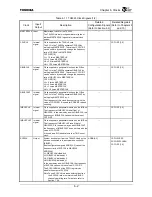
Table 6.1.1 TX4925 Clock Signals (2/2)
Clock
Input/
Output
Description
Related
Configuration Signals
(Refer to Section 3.2)
Related Registers
(Refer to Chapters 5
and 10.)
SDCLK[1:0] Output Clock supplied to SDRAM. The frequency of
SDCLK[1:0] is the same as that of GBUSCLK.
In the same way as with GBUSCLK, the frequency
of SDCLK varies with the value of CCFG.RF.
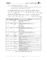
The SDCLKEN[1:0] field of the PCFG register can
disable the output of SDCLK[1:0] on a per bit basis.
⎯
PCFG.SDCLKEN [1:0]
CCFG.RF[1:0]
SDCLKIN Input/output
Reference clock used to latch input data signals
from SDRAM.
The clock output from SDCLK should be connected
to SDCLKIN via a feedback line outside the TX4925.
⎯
⎯
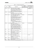
PCICLK[2:1]
Output
Clock supplied to devices on the PCI bus.
The PLL in the TX4925 generates PCICLK by
multiplying MASTERCLK by 5/3.
These clock signals are output when the ADDR[18]
boot configuration signal is set to use the clock
internally generated in the TX4925 as PCICLK.
Otherwise, the pins are placed in High-Z state.
The PCICLKEN bit of the PCFG register can also
disable the output of PCICLK after the reset
sequence is completed.
Note:PCICLK[2:1] can supply clock pulses at 33
MHz when the MASTERCLK frequency is set
to 20 MHz.
ADDR[18] PCFG.PCICLKEN[2:1]
PCICLKIO Input/output
PCI bus clock. The built-in PCI controller of the
TX4925 operates with this clock.
A boot configuration signal (ADDR[18]) can
determine whether the clock internally generated in
the TX4925 is used as PCICLK. If the TX4925
internal clock is selected, the clock signals are
output and simultaneously fed back to the internal
PCI block. When using the PCI block, therefore, do
not set the PCICLK Enable field of the pin
configuration register (PCFG.PCICLKEN[0]) to 0.
ADDR[18] PCFG.PCICLKEN[0]
SCLK Input
Input clock for SIO. SCLK is shared by SIO0 and
SIO1.
The pin is shared with the PIO[5] signal.
⎯
⎯
TCLK Input
Input clock for timers. TCLK is shared by TMR0,
TMR1, and TMR2.
The pin is shared with the PIO[18] signal.
⎯
⎯
BITCLK
Input
Input clock for the AC-link controller.
The pin is shared with the PIO[15] signal.
⎯
⎯
CHICLK
Input/output Clock for the CHI module.
The pin is shared with the PIO[19] signal.
The direction of the clock signal is set using
CHICLOCK.
⎯
CHICLOCK
SPICLK
Output
Output clock for the SPI module.
The pin is shared with the PIO[23] signal.
⎯
⎯
TCK
Input
Input clock for JTAG.
⎯
⎯
DCLK
Output
Clock output for the real-time debugging system.
TDO
⎯
Содержание TMPR4925
Страница 1: ...64 Bit TX System RISC TX49 Family TMPR4925 Rev 3 0 ...
Страница 4: ......
Страница 15: ...Handling Precautions ...
Страница 16: ......
Страница 18: ...1 Using Toshiba Semiconductors Safely 1 2 ...
Страница 40: ...3 General Safety Precautions and Usage Considerations 3 18 ...
Страница 42: ...4 Precautions and Usage Considerations 4 2 ...
Страница 43: ...TMPR4925 ...
Страница 44: ......
Страница 54: ...Chapter 1 Features 1 8 ...
Страница 58: ...Chapter 2 Block Diagram 2 4 ...
Страница 88: ...Chapter 4 Address Mapping 4 12 ...
Страница 226: ...Chapter 8 DMA Controller 8 58 ...
Страница 260: ...Chapter 9 SDRAM Controller 9 34 ...
Страница 480: ...Chapter 15 Interrupt Controller 15 32 ...
Страница 554: ...Chapter 19 Real Time Clock RTC 19 8 ...
Страница 555: ...Chapter 20 Removed 20 1 20 Removed ...
Страница 556: ...Chapter 20 Removed 20 2 ...
Страница 564: ...Chapter 21 Extended EJTAG Interface 21 8 ...
Страница 580: ...Chapter 22 Electrical Characteristics 22 16 ...
Страница 586: ...Chapter 23 Pin Layout Package 23 6 23 2 Package Package Type Package Code 256 pin PBGA PBGA 4L P BGA256 2727 1 27A4 ...
Страница 588: ...Chapter 24 Usage Notes 24 2 ...
Страница 590: ...Appendix A TX49 H2 Core Supplement A 2 ...

