Chapter 10 PCI Controller
10-18
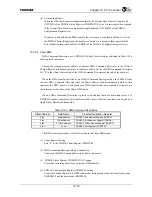
(3) Chain Enable bit checking
Reads the value of the Chain Enable bit (CHNEN) in the PDMAC Configuration Register
(PDMCFG). If the read value is “0”, then the Chain Address field value of the DMA
Command Descriptor indicated by the address stored in the PDMAC Chain Address Register
(PDMCA) is written to the PDMAC Chain Address Register (PDMCA).
10.3.9.4 Data Transfer Mode
The Transfer Mode field in the PDMAC Configuration register (PDMCFG.XFRMODE) selects
a data transfer mode for a DMA transaction over the G-Bus. Transfer data size and when a transfer
is started differ mode by mode.
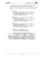
Table 10.3.7 shows the available data transfer modes. Mode 00 performs a single-beat transfer;
Mode 01 performs a burst transfer. In either mode, the PDMAC reads data from the source
address, and after the read cycles are complete, writes the data to the destination address. Source
read and destination write cycles do not overlap.
Table 10.3.7 Data Transfer Modes
G-Bus to the PCI bus
PDMCFG.X
FRMODE
Free FIFO Space
Required for
G-Bus Read
Accesses
(DWORDs)
Number of
DWORDs Read
from the G-Bus
Number of
DWORDs required
in FIFO for PCI
Bus Write
Accesses
Number of
DWORDs Written
to the PCI Bus
Overlaps of PCI
Bus and G-Bus
Cycles
00
1 1 1 1
None
01 16
16
(Burst)
*
1
16 16
(Burst) None
PCI Bus to the G-Bus
PDMCFG.X
FRMODE
Free FIFO Space
Required for
G-Bus Write
Accesses
(DWORDs)
Number of
DWORDs Written
to the G-Bus
Number of
DWORDs
Required in FIFO
for PCI Bus Read
Accesses
Number of
DWORDs Read
from the PCI Bus
Overlaps of PCI
Bus and G-Bus
Cycles
00
1 1 1 1
None
01 16
16
(Burst)
*
1
16 16
(Burst) None
*
1:
The last DMA transfer consists of less than 16 DWORDs if the data to be transferred is not a
multiple of 16 DWORDs.
Note: The amount of data transferred varies, depending on the number of DWORDs present in the
FIFO.
Содержание TMPR4925
Страница 1: ...64 Bit TX System RISC TX49 Family TMPR4925 Rev 3 0 ...
Страница 4: ......
Страница 15: ...Handling Precautions ...
Страница 16: ......
Страница 18: ...1 Using Toshiba Semiconductors Safely 1 2 ...
Страница 40: ...3 General Safety Precautions and Usage Considerations 3 18 ...
Страница 42: ...4 Precautions and Usage Considerations 4 2 ...
Страница 43: ...TMPR4925 ...
Страница 44: ......
Страница 54: ...Chapter 1 Features 1 8 ...
Страница 58: ...Chapter 2 Block Diagram 2 4 ...
Страница 88: ...Chapter 4 Address Mapping 4 12 ...
Страница 226: ...Chapter 8 DMA Controller 8 58 ...
Страница 260: ...Chapter 9 SDRAM Controller 9 34 ...
Страница 480: ...Chapter 15 Interrupt Controller 15 32 ...
Страница 554: ...Chapter 19 Real Time Clock RTC 19 8 ...
Страница 555: ...Chapter 20 Removed 20 1 20 Removed ...
Страница 556: ...Chapter 20 Removed 20 2 ...
Страница 564: ...Chapter 21 Extended EJTAG Interface 21 8 ...
Страница 580: ...Chapter 22 Electrical Characteristics 22 16 ...
Страница 586: ...Chapter 23 Pin Layout Package 23 6 23 2 Package Package Type Package Code 256 pin PBGA PBGA 4L P BGA256 2727 1 27A4 ...
Страница 588: ...Chapter 24 Usage Notes 24 2 ...
Страница 590: ...Appendix A TX49 H2 Core Supplement A 2 ...


