Chapter 10 PCI Controller
10-23
10.3.13 Set Configuration Space
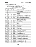
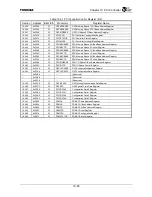
In Table 10.5.1, the values for the registers inside the PCI Configuration Space Register that have a
gray background can be rewritten using one of the following method.
10.3.13.1 Set the Configuration Space Using Software Reset
By using the following procedure, it is possible to use the software to set the configuration
space.
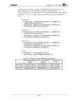
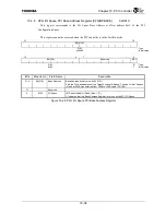
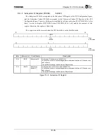
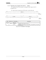
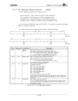
(1) Set the value to be loaded in the Configuration Data 0 Register (PCICDATA0), the
Configuration Data 1 Register (PCICDATA1), the Configuration Data 2 Register
(PCICDATA2), and the Configuration Data 3 Register (PCICDATA3).
(2) Clear the Load Configuration Data Register bit (LCFG) of the PCI Controller Configuration
Register (PCICCFG).
After these processes are complete, please set the Target Configuration Access Ready bit
(PCICCFG.TCAR) of the PCI Controller Configuration Register to be able to accept access to the
PCI Configuration space.
10.3.14 PCI Clock Signal
The configuration setting via ADDR[18] during boot-up determines whether or not the clock from the
on-chip PLL is driven out from the PCI Clock outputs, PCICLK[2:1] and PCICLKIO. When ADDR[18]
is High, PCICLK[2:1] and PCICLKIO are configured as outputs. When ADDR[18] is Low,
PCICLK[2:1] are forced to the High-Z state and PCICLKIO is configured as an input.
When PCICLK[2:1] and PCICLKIO are configured as outputs, the PCFG.PCICLKIOEN bit must not
be cleared. When configured as an output, the PCIC internally feeds back PCICLKIO as a PCI bus
clock to adjust the phase of the clock. However, if the PCFG.PCICLKEN[2:1] and PCFG.PCICLKIOEN
bits are cleared, PCICLK[2:1] and PCICLKIO are held Low respectively. (see Figure 6.1.1).
Содержание TMPR4925
Страница 1: ...64 Bit TX System RISC TX49 Family TMPR4925 Rev 3 0 ...
Страница 4: ......
Страница 15: ...Handling Precautions ...
Страница 16: ......
Страница 18: ...1 Using Toshiba Semiconductors Safely 1 2 ...
Страница 40: ...3 General Safety Precautions and Usage Considerations 3 18 ...
Страница 42: ...4 Precautions and Usage Considerations 4 2 ...
Страница 43: ...TMPR4925 ...
Страница 44: ......
Страница 54: ...Chapter 1 Features 1 8 ...
Страница 58: ...Chapter 2 Block Diagram 2 4 ...
Страница 88: ...Chapter 4 Address Mapping 4 12 ...
Страница 226: ...Chapter 8 DMA Controller 8 58 ...
Страница 260: ...Chapter 9 SDRAM Controller 9 34 ...
Страница 480: ...Chapter 15 Interrupt Controller 15 32 ...
Страница 554: ...Chapter 19 Real Time Clock RTC 19 8 ...
Страница 555: ...Chapter 20 Removed 20 1 20 Removed ...
Страница 556: ...Chapter 20 Removed 20 2 ...
Страница 564: ...Chapter 21 Extended EJTAG Interface 21 8 ...
Страница 580: ...Chapter 22 Electrical Characteristics 22 16 ...
Страница 586: ...Chapter 23 Pin Layout Package 23 6 23 2 Package Package Type Package Code 256 pin PBGA PBGA 4L P BGA256 2727 1 27A4 ...
Страница 588: ...Chapter 24 Usage Notes 24 2 ...
Страница 590: ...Appendix A TX49 H2 Core Supplement A 2 ...

