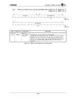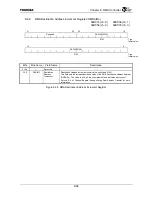
Chapter 8 DMA Controller
8-19
8.3.12 Interrupts
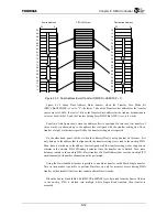
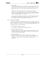
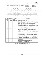
An interrupt number (10 – 13) of the Interrupt Controller is mapped to each channel. In addition,
there are completion interrupts for when transfer ends normally and error interrupts for when transfer
ends abnormally for each channel. When an interrupt occurs, then the bit that corresponds to either the
Normal Interrupt Status field (DIS[3:0]) or the Error Interrupt Status field (EIS[3:0]) of the DMA
Master Control Register (DMMCR) is set.
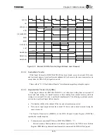
Figure 8.3.6 shows the relationship between the Status bit and Interrupt Enable bit for each interrupt
cause. Refer to the explanation for each Status bit for more information regarding each information
cause.
Figure 8.3.6 DMA Controller Interrupt Signal
8.3.13 Transfer Stall Detection Function
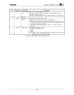
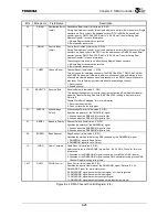
If the period from when a certain channel last performs internal bus access to when the next internal
bus access is performed exceeds the Transfer Stall Detection Interval field (STLTIME) of the DMA
Channel Control Register (DMCCRn), the Transfer Stall Detection bit (STLXFER) of the DMA
Channel Status Register (DMCSRn) is set. An error interrupt is signalled if the Error Interrupt Enable
bit (DMCCRn.INTENE) is set.
In contrast to other error interrupts, DMA transfer is not stopped. Normal DMA transfer is executed if
bus ownership can be obtained. Furthermore, clearing the Transfer Stall Detection (STLXFER)
resumes transfer stall detection as well.
Setting the Transfer Stall Detection Interval field (STLTIME) to “000” disables the Transfer Stall
Detection function.
DMMCR.DIS[n]
DMCSRn.CFERR
DMCSRn.CHERR
DMCSRn.DESERR
DMCSRn.SORERR
DMCSRn.STLXFER
DMMCR.EIS[n]
DMCCRn.INTENE
DMCSRn.NCHNC
DMCCRn.INTENC
DMCSRn.NTRNFC
DMCCRn.INTENT
Interrupt Controller
(Interrupt No. 10 – 13)
DMCSRn.ABCHC
Содержание TMPR4925
Страница 1: ...64 Bit TX System RISC TX49 Family TMPR4925 Rev 3 0 ...
Страница 4: ......
Страница 15: ...Handling Precautions ...
Страница 16: ......
Страница 18: ...1 Using Toshiba Semiconductors Safely 1 2 ...
Страница 40: ...3 General Safety Precautions and Usage Considerations 3 18 ...
Страница 42: ...4 Precautions and Usage Considerations 4 2 ...
Страница 43: ...TMPR4925 ...
Страница 44: ......
Страница 54: ...Chapter 1 Features 1 8 ...
Страница 58: ...Chapter 2 Block Diagram 2 4 ...
Страница 88: ...Chapter 4 Address Mapping 4 12 ...
Страница 226: ...Chapter 8 DMA Controller 8 58 ...
Страница 260: ...Chapter 9 SDRAM Controller 9 34 ...
Страница 480: ...Chapter 15 Interrupt Controller 15 32 ...
Страница 554: ...Chapter 19 Real Time Clock RTC 19 8 ...
Страница 555: ...Chapter 20 Removed 20 1 20 Removed ...
Страница 556: ...Chapter 20 Removed 20 2 ...
Страница 564: ...Chapter 21 Extended EJTAG Interface 21 8 ...
Страница 580: ...Chapter 22 Electrical Characteristics 22 16 ...
Страница 586: ...Chapter 23 Pin Layout Package 23 6 23 2 Package Package Type Package Code 256 pin PBGA PBGA 4L P BGA256 2727 1 27A4 ...
Страница 588: ...Chapter 24 Usage Notes 24 2 ...
Страница 590: ...Appendix A TX49 H2 Core Supplement A 2 ...

