Chapter 16 CHI Module
16-10
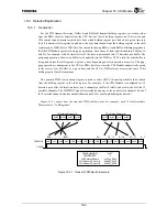
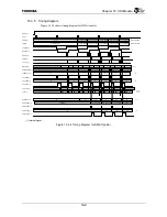
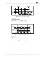
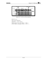
16.3.7 Frame Structure and Serial Timing
Each CHI frame (nominally 8 kHz rate) is time-division-multiplexed into several timeslots or
channels. The total number of timeslots per frame is programmable, with a maximum of 64 timeslots
allowed, and the number of timeslots is also restricted to an even number. Each timeslot is 8 bits,
although 16-bit or 32-bit channels can be supported by accessing adjacent timeslots.
The TX4925 CHI Module supports a master or slave mode for both the clock (CHICLK) and sync
(CHIFS). For the master mode, the TX4925 contains programmable dividers for generating the clock
and/or sync signal, synchronously dividing down from the main core clock (CLK). For the slave mode,
TX4925 accepts external clock and/or sync signals and utilizes “digital-PLL” type circuitry to stayed
“locked” to the external source.
The CHI Module supports the following programmable features which allow support for various
clock and sync timing formats:
1x versus 2x clock modes for CHICLK (2x clock mode uses two CHICLK periods per data bit)
MSB-first versus LSB-first serial formats for transmit and receive
rising versus falling edge (polarity) used for frame sync triggering
CHIFS signal can be sampled on either rising or falling edge of CHICLK
CHIDIN receive data can be sampled on either rising or falling edge of CHICLK
CHIDOUT transmit data can be pushed on either rising or falling edge of CHICLK
CHIDIN receive data can have programmable bit offset (timeslot 0 offset from CHIFS)
CHIDOUT transmit data can have programmable bit offset (timeslot 0 offset from CHIFS)
CHIDOUT transmit data (tri-state) output buffer enable is dynamically asserted for only active
timeslots; for sleep mode CHIDOUT is always tri-stated
for CHIFS master mode, the CHIFS pulse width and polarity is programmable
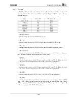
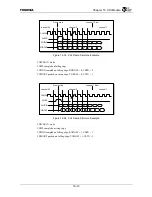
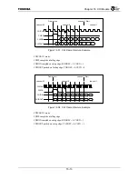
The TX4925 CHI Module allows for a programmable bit offset for both CHIDIN and CHIDOUT,
which is related to the number of clock cycles between the start of timeslot 0 and CHIFS. This
flexibility allows the TX4925 CHI Module to support a wide variety of interface clock and sync timing
formats. The control bits for controlling the CHIDIN bit offset are CHIRXBOFF[3:0], while the control
bits for controlling the CHIDOUT bit offset are CHITXBOFF[3:0].
Содержание TMPR4925
Страница 1: ...64 Bit TX System RISC TX49 Family TMPR4925 Rev 3 0 ...
Страница 4: ......
Страница 15: ...Handling Precautions ...
Страница 16: ......
Страница 18: ...1 Using Toshiba Semiconductors Safely 1 2 ...
Страница 40: ...3 General Safety Precautions and Usage Considerations 3 18 ...
Страница 42: ...4 Precautions and Usage Considerations 4 2 ...
Страница 43: ...TMPR4925 ...
Страница 44: ......
Страница 54: ...Chapter 1 Features 1 8 ...
Страница 58: ...Chapter 2 Block Diagram 2 4 ...
Страница 88: ...Chapter 4 Address Mapping 4 12 ...
Страница 226: ...Chapter 8 DMA Controller 8 58 ...
Страница 260: ...Chapter 9 SDRAM Controller 9 34 ...
Страница 480: ...Chapter 15 Interrupt Controller 15 32 ...
Страница 554: ...Chapter 19 Real Time Clock RTC 19 8 ...
Страница 555: ...Chapter 20 Removed 20 1 20 Removed ...
Страница 556: ...Chapter 20 Removed 20 2 ...
Страница 564: ...Chapter 21 Extended EJTAG Interface 21 8 ...
Страница 580: ...Chapter 22 Electrical Characteristics 22 16 ...
Страница 586: ...Chapter 23 Pin Layout Package 23 6 23 2 Package Package Type Package Code 256 pin PBGA PBGA 4L P BGA256 2727 1 27A4 ...
Страница 588: ...Chapter 24 Usage Notes 24 2 ...
Страница 590: ...Appendix A TX49 H2 Core Supplement A 2 ...


