Chapter 14 AC-link Controller
14-12
14.3.6.4 DMA Operation
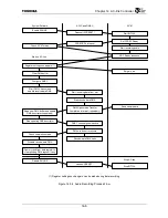
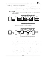
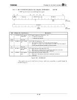
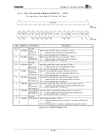
When ACLC’s REQ latch (refer to Figure 14.3.6 and Figure 14.3.7) needs to read or write
sample-data, it issues a DMA request. When DMAC acknowledges the request by performing
write- or read-access to the ACLC sample-data register, ACLC deasserts the request. Therefore,
the software must properly set up DMAC so that the source or destination points to the
corresponding sample-data register for the DMA channel.
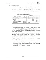
Setup the DMA Channel Control Registers (DMCCRn) in DMAC as follows.
Immediate chain
Enable
DMCCRn.IMMCHN = 1 [Note]
DMA request polarity
Low-active
DMCCRn.REQPOL = 0
DMA acknowledge polarity
Low-active DMCCRn.ACKPOL
=
0
Request sense
Level-sensitive
DMCCRn.EGREQ = 0
Simple chain
Enable
DMCCRn.SMPCHN = 1
Transfer size
1 word
DMCCRn.XFSZ = 010b
Transfer address mode
Dual
DMCCRn.SNGAD = 0
Note: Use this setting when DMA chain operation is utilized
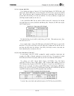
For a transmission channel, assign the address of ACLC Audio PCM
Output/Surround/Center/LFE/Modem Output Register
(ACAUDO/SURR/CENT/LFE/MODODAT) to the DMAC destination address register
(DMDARn). For a reception channel, assign the address of ACLC Audio input/Modem Input
Register (ACAUDI/MODIDAT) to the DMAC source address register (DMSARn).
When any DMA request is pending, the REQ latch will not deasserted the request until the
corresponding sample-data register is accessed. Just unsetting ACLC Control Enable Register
(ACCTLEN)’s DMA Enable (xxxxDMA) bit corresponding to the DMA will not clear the REQ
latch.
The procedure to continuously push or pull the sample-data stream through the chain DMA
operation follows the DMAC specification. Refer to section 8.3.10 for this respect.
Содержание TMPR4925
Страница 1: ...64 Bit TX System RISC TX49 Family TMPR4925 Rev 3 0 ...
Страница 4: ......
Страница 15: ...Handling Precautions ...
Страница 16: ......
Страница 18: ...1 Using Toshiba Semiconductors Safely 1 2 ...
Страница 40: ...3 General Safety Precautions and Usage Considerations 3 18 ...
Страница 42: ...4 Precautions and Usage Considerations 4 2 ...
Страница 43: ...TMPR4925 ...
Страница 44: ......
Страница 54: ...Chapter 1 Features 1 8 ...
Страница 58: ...Chapter 2 Block Diagram 2 4 ...
Страница 88: ...Chapter 4 Address Mapping 4 12 ...
Страница 226: ...Chapter 8 DMA Controller 8 58 ...
Страница 260: ...Chapter 9 SDRAM Controller 9 34 ...
Страница 480: ...Chapter 15 Interrupt Controller 15 32 ...
Страница 554: ...Chapter 19 Real Time Clock RTC 19 8 ...
Страница 555: ...Chapter 20 Removed 20 1 20 Removed ...
Страница 556: ...Chapter 20 Removed 20 2 ...
Страница 564: ...Chapter 21 Extended EJTAG Interface 21 8 ...
Страница 580: ...Chapter 22 Electrical Characteristics 22 16 ...
Страница 586: ...Chapter 23 Pin Layout Package 23 6 23 2 Package Package Type Package Code 256 pin PBGA PBGA 4L P BGA256 2727 1 27A4 ...
Страница 588: ...Chapter 24 Usage Notes 24 2 ...
Страница 590: ...Appendix A TX49 H2 Core Supplement A 2 ...


