Chapter 11 Serial I/O Port
11-7
11.3.4 Data
Reception
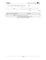
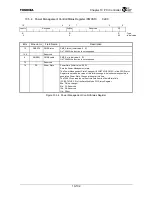
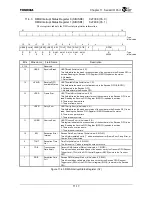
When the Serial Data Reception Disable bit (RSDE) of the Flow Control Register (SIFLCRn) is set
to “0”, reception operation starts after the RXD signal start bit is detected. Start bits are detected when
the RXD signal transitions from the High state to the Low state. Therefore, the RXD signal is not
interpreted as a start bit if it is Low when the Serial Data Reception Disable bit is set to “0”.
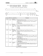
The received data are stored in the Receive FIFO. The Reception Data Full bit (RDIS) of the
DMA/Interrupt Status Register (SIDISRn) is set if the byte count of the stored reception data exceeds
the value set by the Receive FIFO Request Trigger Level field (RDIL) of the FIFO Control Register
(SIFCRn).
An interrupt is signaled when the Reception Data Interrupt Enable bit (RIE) of the DMA/Interrupt
Control Register (SIDICRn) is set. The received data can be read from the Receive FIFO Data Register
(SIRFIFOn).
In addition, DMA transfer is initiated when the Reception Data DMA Enable bit (RDE) of the
DMA/Interrupt Control Register (SIDICRn) is set.
11.3.5 Data
Transmission
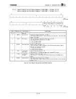
Data stored in the Transmission Data FIFO are transmitted when the Serial Data Transmission
Disable bit (TSDE) of the Flow Control Register (SIFLCRn) is set to “0”.
If the available space in the Transmit FIFO is greater than the byte count set by the Transmit FIFO
Request Trigger Level (TDIL) of the Control Register (SIFCRn), the transmission data empty bit
(TDIS) of the DMA/Interrupt Status Register (SIDISRn) is set.
An interrupt is signaled when the Transmission Data Interrupt Enable bit (TIE) of the DMA/Interrupt
Control Register (SIDICRn) is set.
In addition, DMA transfer is initiated when the Transmission Data DMA Enable bit (TDE) of the
DMA/Interrupt Control Register (SIDICRn) is set.
Содержание TMPR4925
Страница 1: ...64 Bit TX System RISC TX49 Family TMPR4925 Rev 3 0 ...
Страница 4: ......
Страница 15: ...Handling Precautions ...
Страница 16: ......
Страница 18: ...1 Using Toshiba Semiconductors Safely 1 2 ...
Страница 40: ...3 General Safety Precautions and Usage Considerations 3 18 ...
Страница 42: ...4 Precautions and Usage Considerations 4 2 ...
Страница 43: ...TMPR4925 ...
Страница 44: ......
Страница 54: ...Chapter 1 Features 1 8 ...
Страница 58: ...Chapter 2 Block Diagram 2 4 ...
Страница 88: ...Chapter 4 Address Mapping 4 12 ...
Страница 226: ...Chapter 8 DMA Controller 8 58 ...
Страница 260: ...Chapter 9 SDRAM Controller 9 34 ...
Страница 480: ...Chapter 15 Interrupt Controller 15 32 ...
Страница 554: ...Chapter 19 Real Time Clock RTC 19 8 ...
Страница 555: ...Chapter 20 Removed 20 1 20 Removed ...
Страница 556: ...Chapter 20 Removed 20 2 ...
Страница 564: ...Chapter 21 Extended EJTAG Interface 21 8 ...
Страница 580: ...Chapter 22 Electrical Characteristics 22 16 ...
Страница 586: ...Chapter 23 Pin Layout Package 23 6 23 2 Package Package Type Package Code 256 pin PBGA PBGA 4L P BGA256 2727 1 27A4 ...
Страница 588: ...Chapter 24 Usage Notes 24 2 ...
Страница 590: ...Appendix A TX49 H2 Core Supplement A 2 ...

