Chapter 5 Configuration Register
5-3
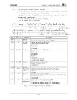
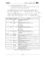
5.2.1 Chip
Configuration
Register (CCFG) 0xE000
For the bit fields whose initial values are set by boot configuration (refer to Section 3.2), the initial
input signal level and the corresponding register value are indicated.
The following bits are Reserved (Read only). An explanation of the type and default was added so the
default is reflected in the Boot signal.
bit 31: R
~
ADDR[10], bit 28: R UAE, bit 27: R ADDR[16]
bit 18: R ADDR[17], bit 12: R ADDR[19]
31
27 26 25 24 23 21 20 19 18 17 16
Reserved
Reserved
RF BOOTME
PCIMODE
Reserved
TINTDIS BEOW
R/W R/W
R
R R
R/W1C
: Type
0
0
ADDR[8:6]
ADDR[15]
ADDR[0]
0
: Initial value
15
14
13
12 8 7 6 5 4 3 2 1 0
WR TOE
PCIARB
Reserved SYSSP
Reserved
PCTRCE
ENDIAN WDRST
UAEHOLD
R/W
R/W
R
R
R/W R
R
R/W1C
R/W :
Type
0
0
~ADDR[1]
ADDR[4:3] 11 ~TDO
ADDR[14]
0 1
:
Initial
value
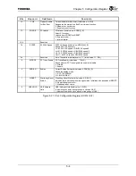
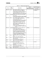
Bits Mnemonic Field
Name
Description
31:27
⎯
Reserved
⎯
26
⎯
Reserved
Note: This bit is always set to “0”. (Initial value: 0, R/W)
25:24 RF
Reduced
Frequency
Reduced Frequency (Initial value: 00, R/W)
These bits select the internal bus speed.
00: full speed
01: 1/2 speed
10: 1/4 speed
11: 1/8 speed
23:21 BOOTME
Boot
Memory Boot Memory (Initial value: ADDR[8:6], R)
Shows Boot Memory
000: Reserved
001: Reserved
010: Reserved
011: PCIC
100: Reserved
101: EBUSC ch0 at third speed
110: EBUSC ch0 at half speed
111: EBUSC ch0 at full speed
20 PCIMODE
PCI
Mode PCI Mode (Initial value: ADDR[15], R)
Shows the PCI operation mode.
L: Satellite mode
H: Host mode
19:18
⎯
Reserved
⎯
17 TINTDIS
TX49/H2 core
Timer Interrupt
Disable
TX49/H2 core Timer Interrupt Disable (Initial value: ADDR[0], R)
Shows whether TX49/H2 core Timer Interrupt is enable or disable.
L: Enable
H: Disable
16 BEOW
Bus Error on
Write
Bus Error on Write (Initial value: 0, R/W1C)
Indicates that a bus error was generated by a write operation of the TX49/H2 Core.
Writing a “1” clears the bit.
0: No error occur
1: Error occurs
15
WR
Watchdog Timer
for Reset/NMI
Watchdog Timer for Reset/NMI (Initial value: 0, R/W)
Designates the connection of the Watchdog Timer.
0: Watchdog Timer Interrupt is connected to TX4925 internal NMI
*
.
1: Watchdog Timer Interrupt is connected to TX4925 internal Reset.
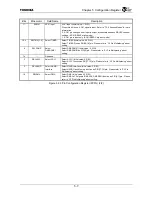
Figure 5.2.1 Chip Configuration Register (CCFG)
(1/2)
Содержание TMPR4925
Страница 1: ...64 Bit TX System RISC TX49 Family TMPR4925 Rev 3 0 ...
Страница 4: ......
Страница 15: ...Handling Precautions ...
Страница 16: ......
Страница 18: ...1 Using Toshiba Semiconductors Safely 1 2 ...
Страница 40: ...3 General Safety Precautions and Usage Considerations 3 18 ...
Страница 42: ...4 Precautions and Usage Considerations 4 2 ...
Страница 43: ...TMPR4925 ...
Страница 44: ......
Страница 54: ...Chapter 1 Features 1 8 ...
Страница 58: ...Chapter 2 Block Diagram 2 4 ...
Страница 88: ...Chapter 4 Address Mapping 4 12 ...
Страница 226: ...Chapter 8 DMA Controller 8 58 ...
Страница 260: ...Chapter 9 SDRAM Controller 9 34 ...
Страница 480: ...Chapter 15 Interrupt Controller 15 32 ...
Страница 554: ...Chapter 19 Real Time Clock RTC 19 8 ...
Страница 555: ...Chapter 20 Removed 20 1 20 Removed ...
Страница 556: ...Chapter 20 Removed 20 2 ...
Страница 564: ...Chapter 21 Extended EJTAG Interface 21 8 ...
Страница 580: ...Chapter 22 Electrical Characteristics 22 16 ...
Страница 586: ...Chapter 23 Pin Layout Package 23 6 23 2 Package Package Type Package Code 256 pin PBGA PBGA 4L P BGA256 2727 1 27A4 ...
Страница 588: ...Chapter 24 Usage Notes 24 2 ...
Страница 590: ...Appendix A TX49 H2 Core Supplement A 2 ...

