Chapter 10 PCI Controller
10-1
10. PCI
Controller
10.1 Features
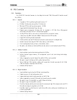
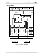
The TX4925 PCI Controller functions as a bus bridge between the TX4925 External PCI and the internal
bus (G-Bus).
10.1.1 Overall
•
Compliant to “PCI Local Bus Specification Revision 2.2”
•
PCI Bus: 32-bit data bus; Internal Bus: 32-bit data bus
•
Maximum PCI bus clock operating frequency: 33 MHz
•
Supports both the Initiator and Target functions
•
Supports power management functions that are compliant to PCI Bus Power Management
Interface Specifications Version 1.1 (Partially unsupported).
•
On-chip PCI Bus Arbiter, can connect to a maximum of four external bus masters
•
1-channel on-chip DMA Controller (PDMAC) dedicated to the PCI Controller
•
Supports PCI clock input mode/output mode
•
The Internal Bus clock and PCI Bus clock are asynchronous and can be set independently
•
Includes function for booting the TX4925 from memory on the PCI Bus
•
Can set configuration data by software at the initialize routine
•
Mounted a retry function on the Internal Bus side also in order to avoid deadlock on the PCI Bus.
10.1.2 Initiator
Function
•
Single and Burst transfer from the Internal Bus to the PCI Bus
•
Initiator function Supports memory, I/O, configuration, special cycle, and interrupt acknowledge
transactions.
•
Address mapping between the Internal Bus and the PCI Bus can be modified
•
Mounted 8-stage 32-bit data one FIFO each for Read and Write
•
Indirect Read and Write function enables quick termination of single transactions by the G-Bus
without waiting for completion on the PCI Bus.
•
Endian switching function
10.1.3 Target
Function
•
Single and Burst transfer from the PCI Bus to the Internal Bus
•
Supports memory, I/O, and configuration cycles
•
Supports high-speed back-to-back transactions on the PCI Bus
•
Address mapping between the PCI Bus and the Internal bus can be modified
•
Mounted 32-stage 32-bit data FIFO on each PCI Channel for Read
•
Mounted 16-stage 32-bit data FIFO for Write
•
Post Write function enables quick termination of a maximum of eight Write transactions by the PCI
Bus without waiting for completion on the G-Bus.
•
Read Burst length (pre-fetch data size) on the Internal Bus when reading a pre-fetchable space can
be made programmable
•
Endian switching function
Содержание TMPR4925
Страница 1: ...64 Bit TX System RISC TX49 Family TMPR4925 Rev 3 0 ...
Страница 4: ......
Страница 15: ...Handling Precautions ...
Страница 16: ......
Страница 18: ...1 Using Toshiba Semiconductors Safely 1 2 ...
Страница 40: ...3 General Safety Precautions and Usage Considerations 3 18 ...
Страница 42: ...4 Precautions and Usage Considerations 4 2 ...
Страница 43: ...TMPR4925 ...
Страница 44: ......
Страница 54: ...Chapter 1 Features 1 8 ...
Страница 58: ...Chapter 2 Block Diagram 2 4 ...
Страница 88: ...Chapter 4 Address Mapping 4 12 ...
Страница 226: ...Chapter 8 DMA Controller 8 58 ...
Страница 260: ...Chapter 9 SDRAM Controller 9 34 ...
Страница 480: ...Chapter 15 Interrupt Controller 15 32 ...
Страница 554: ...Chapter 19 Real Time Clock RTC 19 8 ...
Страница 555: ...Chapter 20 Removed 20 1 20 Removed ...
Страница 556: ...Chapter 20 Removed 20 2 ...
Страница 564: ...Chapter 21 Extended EJTAG Interface 21 8 ...
Страница 580: ...Chapter 22 Electrical Characteristics 22 16 ...
Страница 586: ...Chapter 23 Pin Layout Package 23 6 23 2 Package Package Type Package Code 256 pin PBGA PBGA 4L P BGA256 2727 1 27A4 ...
Страница 588: ...Chapter 24 Usage Notes 24 2 ...
Страница 590: ...Appendix A TX49 H2 Core Supplement A 2 ...

