Chapter 8 DMA Controller
8-10
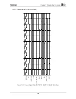
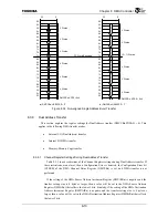
(a) DMCCRn.USEXFSZ
=
“0”
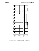
(b) DMCCRn.USEXFSZ
=
“1”
Figure 8.3.2 Non-aligned Single Address Burst Transfer
8.3.8 Dual
Address
Transfer
This section explains the register settings for Dual Address transfer (DMCCRn.SNGAD = 0). This
applies to the following DMA transfer modes.
•
External I/O (Dual Address) transfer
•
Internal I/O DMA transfer
•
Memory-Memory Copy transfer
8.3.8.1
Channel Register Settings During Dual Address Transfer
Table 8.3.3 shows restrictions of the Channel Register settings during Dual Address transfer. If
these restrictions are not met, then a Configuration Error is detected, the Configuration Error bit
(CFERR) of the DMA Channel Status Register (DMCSRn) is set, and DMA transfer is not
performed.
If the setting of the DMA Source Address Increment Register (DMSAIRn) is negative and the
transfer setting size is 4 bytes or larger, then a value will be set in the DMA Source Address
Register (DMSARn) that reflects the lower 2 bits. Similarly, if the setting of the DMA Destination
Address Increment Register (DMDAIRn) is negative and the transfer setting size is 4 bytes or
larger, then a value will be set in the DMA Destination Address Register (DMDARn) that reflects
the lower 2 bits.
50
54
58
5c
64
68
6c
60
74
78
7c
70
00
04
08
0c
14
18
1c
10
24
28
2c
20
30
3 Words
4 Words
4 Words
4 Words
4 Words
4 Words
DMCCRn.XFSZ
=
0x4
32 Word Boundary
32
0
50
54
58
5c
64
68
6c
60
74
78
7c
70
00
04
08
0c
14
18
1c
10
24
28
2c
20
30
4 Words
4 Words
(3
+
1) Words
4 Words
4 Words
DMCCRn. XFSZ
=
0x4
32
0
4 Words
Содержание TMPR4925
Страница 1: ...64 Bit TX System RISC TX49 Family TMPR4925 Rev 3 0 ...
Страница 4: ......
Страница 15: ...Handling Precautions ...
Страница 16: ......
Страница 18: ...1 Using Toshiba Semiconductors Safely 1 2 ...
Страница 40: ...3 General Safety Precautions and Usage Considerations 3 18 ...
Страница 42: ...4 Precautions and Usage Considerations 4 2 ...
Страница 43: ...TMPR4925 ...
Страница 44: ......
Страница 54: ...Chapter 1 Features 1 8 ...
Страница 58: ...Chapter 2 Block Diagram 2 4 ...
Страница 88: ...Chapter 4 Address Mapping 4 12 ...
Страница 226: ...Chapter 8 DMA Controller 8 58 ...
Страница 260: ...Chapter 9 SDRAM Controller 9 34 ...
Страница 480: ...Chapter 15 Interrupt Controller 15 32 ...
Страница 554: ...Chapter 19 Real Time Clock RTC 19 8 ...
Страница 555: ...Chapter 20 Removed 20 1 20 Removed ...
Страница 556: ...Chapter 20 Removed 20 2 ...
Страница 564: ...Chapter 21 Extended EJTAG Interface 21 8 ...
Страница 580: ...Chapter 22 Electrical Characteristics 22 16 ...
Страница 586: ...Chapter 23 Pin Layout Package 23 6 23 2 Package Package Type Package Code 256 pin PBGA PBGA 4L P BGA256 2727 1 27A4 ...
Страница 588: ...Chapter 24 Usage Notes 24 2 ...
Страница 590: ...Appendix A TX49 H2 Core Supplement A 2 ...


