Chapter 10 PCI Controller
10-46
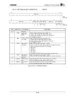
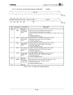
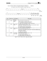
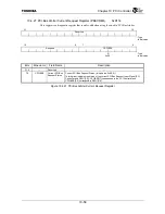
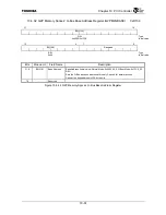
10.4.19 P2G Status Register (P2GSTATUS)
0xD094
31
16
Reserved
:
Type
: Initial value
15
5
4
3
2
1
0
Reserved TOBFE TIBFE PMSC
PERR
GBE
R
R
R/W1C
R/W1C
R/W1C :
Type
1
1
0
0
0
:
Initial
value
Bits Mnemonic Field
Name
Description
31:5
⎯
Reserved
⎯
4 TOBFE
Target Out-Bound
FIFO Empty
Target Out-Bound FIFO Empty (Initial value: 1, R)
1: Indicates that the Target Out-Bound FIFO is empty.
0: Indicates that the Target Out-Bound FIFO is not empty.
This is a diagnostic function.
3 TIBFE
Target In-Bound
FIFO Empty
Target In-Bound FIFO Empty (Initial value: 1, R)
1: Indicates that the Target In-Bound FIFO is empty.
0: Indicates that the Target In-Bound FIFO is not empty.
This is a diagnostic function.
2 PMSC
PM State Change
Detected
Power Management State Change (Initial value: 0, R/W1C)
“1” is set to this bit when the PowerState field of the Power Management Register
(PMCSR) is rewritten.
This bit is cleared to “0” when a “1” is written to it. This bit is only valid when the PCI
Controller is in the Satellite mode.
1 PERR
PERR
*
Detected
PERR
*
Occurred (Initial value: 0, R/W1C)
Indicates that a Parity error occurred during Target access.
1: Indicates that a Parity error occurred.
0: Indicates that no Parity error has occurred..
0 TGBE
Target G-Bus
Error Detect
Target G-Bus Error Detect (Initial value: 0, R/W1C)
Indicates that a G-Bus Error occurred when the G-Bus was Target of the PCI cycle.
This error is indicated when a timeout occurs on the G-Bus. This bit is only set during
PCI Target cycle Bus Errors.
1: Indicates that a G-Bus Error was detected.
0: Indicates that no G-Bus Error was detected.
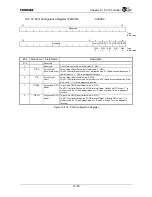
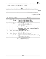
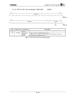
Figure 10.4.19 P2G Status Register
Содержание TMPR4925
Страница 1: ...64 Bit TX System RISC TX49 Family TMPR4925 Rev 3 0 ...
Страница 4: ......
Страница 15: ...Handling Precautions ...
Страница 16: ......
Страница 18: ...1 Using Toshiba Semiconductors Safely 1 2 ...
Страница 40: ...3 General Safety Precautions and Usage Considerations 3 18 ...
Страница 42: ...4 Precautions and Usage Considerations 4 2 ...
Страница 43: ...TMPR4925 ...
Страница 44: ......
Страница 54: ...Chapter 1 Features 1 8 ...
Страница 58: ...Chapter 2 Block Diagram 2 4 ...
Страница 88: ...Chapter 4 Address Mapping 4 12 ...
Страница 226: ...Chapter 8 DMA Controller 8 58 ...
Страница 260: ...Chapter 9 SDRAM Controller 9 34 ...
Страница 480: ...Chapter 15 Interrupt Controller 15 32 ...
Страница 554: ...Chapter 19 Real Time Clock RTC 19 8 ...
Страница 555: ...Chapter 20 Removed 20 1 20 Removed ...
Страница 556: ...Chapter 20 Removed 20 2 ...
Страница 564: ...Chapter 21 Extended EJTAG Interface 21 8 ...
Страница 580: ...Chapter 22 Electrical Characteristics 22 16 ...
Страница 586: ...Chapter 23 Pin Layout Package 23 6 23 2 Package Package Type Package Code 256 pin PBGA PBGA 4L P BGA256 2727 1 27A4 ...
Страница 588: ...Chapter 24 Usage Notes 24 2 ...
Страница 590: ...Appendix A TX49 H2 Core Supplement A 2 ...

