Chapter 17 Serial Peripheral Interface
17-7
17.3.6 SPI
Buffer
Structure
The SPI has both transmit and receive buffer. The buffers are implemented as FIFO and are able to
store four frames each.
When a new SPI transfer is started by writing the data register, the transfer value is first stored in
SPI’s transmit buffer. From there the value will be fetched by the shift register immediately, if the
module is idle or after the currently running transfer has completed.
A receive value from the shift register is stored in the receive buffer every time a transfer completes.
The SPI is able to generate interrupts depending on the fill-level of these buffers. Therefore, it is
possible to refill the buffers with several values within one interrupt service routine, if desired.
17.3.7 SPI System Errors
SPI is able to detect the following system error during the transfer.
17.3.7.1 Overrun Error (SPOE)
An Overrun Error will be generated, when the transmit buffer is completely filled, while a new
value has been written on the SPI Transmit FIFO. In this case the already written data in the
transmit buffer is not changed and the new value is abandoned. Then the SPOE flag in the SPSR
register is set.
17.3.8 Interrupts
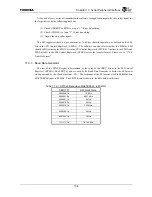
The SPI has three types interrupt sources. OR signal of them connects to the internal Interrupt
Controller (IRC). Please check SPI Status Register (SPSR) to know which type interrupt occurred.
Type Status
Bits
Mask-able
Bit
System error or idle
SPOE, SIDLE
SPOIE, SILIE
Receive Buffer Fill
RBSI
RBFIE
Transmit Buffer Fill
TBSI
TBFIE
The System error or idle interrupt is used for error detection purpose and idle state interrupt. The
receive buffer fill interrupt and the transmit buffer fill interrupt are used to fetch and setup new data in
an interrupt service routine.
Содержание TMPR4925
Страница 1: ...64 Bit TX System RISC TX49 Family TMPR4925 Rev 3 0 ...
Страница 4: ......
Страница 15: ...Handling Precautions ...
Страница 16: ......
Страница 18: ...1 Using Toshiba Semiconductors Safely 1 2 ...
Страница 40: ...3 General Safety Precautions and Usage Considerations 3 18 ...
Страница 42: ...4 Precautions and Usage Considerations 4 2 ...
Страница 43: ...TMPR4925 ...
Страница 44: ......
Страница 54: ...Chapter 1 Features 1 8 ...
Страница 58: ...Chapter 2 Block Diagram 2 4 ...
Страница 88: ...Chapter 4 Address Mapping 4 12 ...
Страница 226: ...Chapter 8 DMA Controller 8 58 ...
Страница 260: ...Chapter 9 SDRAM Controller 9 34 ...
Страница 480: ...Chapter 15 Interrupt Controller 15 32 ...
Страница 554: ...Chapter 19 Real Time Clock RTC 19 8 ...
Страница 555: ...Chapter 20 Removed 20 1 20 Removed ...
Страница 556: ...Chapter 20 Removed 20 2 ...
Страница 564: ...Chapter 21 Extended EJTAG Interface 21 8 ...
Страница 580: ...Chapter 22 Electrical Characteristics 22 16 ...
Страница 586: ...Chapter 23 Pin Layout Package 23 6 23 2 Package Package Type Package Code 256 pin PBGA PBGA 4L P BGA256 2727 1 27A4 ...
Страница 588: ...Chapter 24 Usage Notes 24 2 ...
Страница 590: ...Appendix A TX49 H2 Core Supplement A 2 ...


