Chapter 10 PCI Controller
10-39
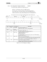
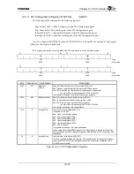
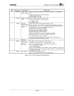
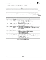
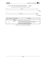
10.4.13 G2P Configuration Register (G2PCFG)
0xD060
31
16
Reserved
:
Type
: Initial value
15 12
11
10 9 8 7 6 5 4 3 2 1 0
Reserved
BSWAPM0 BSWAPM1
BSWAPM2 BSWAPIO G2PM0EN G2PM1EN G2PM2EN
G2PIOEN
IRBER
Reserved BSWAPI
ASERR
R/W R/W R/W R/W R/W R/W R/W R/W R/W
R/W
R/W1C :
Type
0/1
0/1
0/1
0/1
0
0
0
0
1
0/1
0
:
Initial
value
Bits Mnemonic Field
Name
Description
31:12
⎯
Reserved
⎯
11 BSWAPM0
Byte Swap for
Memory Space 0
Byte Swap Disable for Memory Space 0
(Initial value: Little Endian Mode: 0; Big Endian Mode: 1, R/W)
Sets the byte swapping of Memory Space 0.
0: Do not perform byte swapping.
1: Perform byte swapping.
Please use the default state in most situations. If this bit is changed to “0” when in the
Big Endian Mode, the byte order of transfer to Memory Space 0 through DWORD (32-
bit) access will not change.
10 BSWAPM1
Byte Swap for
Memory Space 1
Byte Swap Disable for Memory Space 1
(Initial value: Little Endian Mode: 0; Big Endian Mode: 1, R/W)
Sets the byte swapping of Memory Space 1.
0: Do not perform byte swapping.
1: Perform byte swapping.
Please use the default state in most situations. If this bit is changed to "0” when in the
Big Endian Mode, the byte order of transfer to Memory Space 1 through DWORD (32-
bit) access will not change.
9 BSWAPM2
Byte Swap for
Memory Space 2
Byte Swap Disable for Memory Space 2
(Initial value: Little Endian Mode: 0; Big Endian Mode: 1, R/W)
Sets the byte swapping of Memory Space 2.
0: Do not perform byte swapping.
1: Perform byte swapping.
Please use the default state in most situations. If this bit is changed to “0” when in the
Big Endian Mode, the byte order of transfer to Memory Space 2 through DWORD (32-
bit) access will not change.
8 BSWAPIO
Byte Swap for I/O
Space
Byte Swap Disable for I/O Space
(Initial value: Little Endian Mode: 0; Big Endian Mode: 1, R/W)
Sets the byte swapping of I/O Space.
0: Do not perform byte swapping.
1: Perform byte swapping.
Please use the default state in most situations. If this bit is changed to “0” when in the
Big Endian Mode, the byte order of transfer to I/O Space through DWORD (32-bit)
access will not change.
7 G2PM0EN
Initiator
Memory
Space 0 Enable
Initiator Memory Space 0 Enable (Initial value: 0, R/W)
Controls PCI initiator access to Memory Space 0.
1: Memory Space 0 is valid.
0: Memory Space 0 is invalid.
6 G2PM1EN
Initiator Memory
Space 1 Enable
Initiator Memory Space 1 Enable (Initial value: 0, R/W)
Controls PCI initiator access to Memory Space 1.
1: Memory Space 1 is valid.
0: Memory Space 1 is invalid.
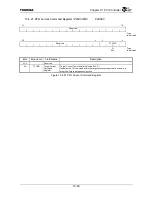
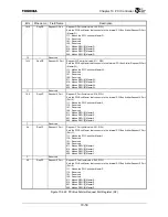
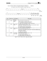
Figure 10.4.13 G2P Configuration Register (1/2)
Содержание TMPR4925
Страница 1: ...64 Bit TX System RISC TX49 Family TMPR4925 Rev 3 0 ...
Страница 4: ......
Страница 15: ...Handling Precautions ...
Страница 16: ......
Страница 18: ...1 Using Toshiba Semiconductors Safely 1 2 ...
Страница 40: ...3 General Safety Precautions and Usage Considerations 3 18 ...
Страница 42: ...4 Precautions and Usage Considerations 4 2 ...
Страница 43: ...TMPR4925 ...
Страница 44: ......
Страница 54: ...Chapter 1 Features 1 8 ...
Страница 58: ...Chapter 2 Block Diagram 2 4 ...
Страница 88: ...Chapter 4 Address Mapping 4 12 ...
Страница 226: ...Chapter 8 DMA Controller 8 58 ...
Страница 260: ...Chapter 9 SDRAM Controller 9 34 ...
Страница 480: ...Chapter 15 Interrupt Controller 15 32 ...
Страница 554: ...Chapter 19 Real Time Clock RTC 19 8 ...
Страница 555: ...Chapter 20 Removed 20 1 20 Removed ...
Страница 556: ...Chapter 20 Removed 20 2 ...
Страница 564: ...Chapter 21 Extended EJTAG Interface 21 8 ...
Страница 580: ...Chapter 22 Electrical Characteristics 22 16 ...
Страница 586: ...Chapter 23 Pin Layout Package 23 6 23 2 Package Package Type Package Code 256 pin PBGA PBGA 4L P BGA256 2727 1 27A4 ...
Страница 588: ...Chapter 24 Usage Notes 24 2 ...
Страница 590: ...Appendix A TX49 H2 Core Supplement A 2 ...

