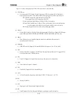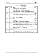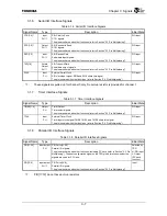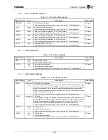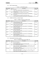
Chapter 3 Signals
3-9
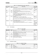
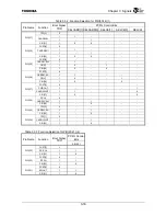
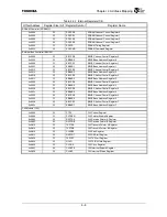
3.1.12 SPI Interface Signals
Table 3.1.12 SPI Interface Signals
Signal Name
Type
Description
Initial State
SPICLK Output
PU
SPI Clock
This pin is used for a data clock to or from an SPI slave device.
The pin is shared with other functions (refer to Section "3.3 Pin Multiplexing").
PIO input
SPIOUT Output
PU
SPI Data Output
This signal contains data to be shifted to an SPI slave device.
The pin is shared with other functions (refer to Section "3.3 Pin Multiplexing").
PIO input
SPIIN Input
PU
SPI Data Input
This signal contains data to be shifted from an SPI slave device.
The pin is shared with other functions (refer to Section "3.3 Pin Multiplexing").
PIO input
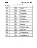
3.1.13 NAND Flash Memory Interface Signals
Table 3.1.13 NAND Flash Memory Interface Signals
Signal Name
Type
Description
Initial State
ND_ALE
Output
NAND Flash Address Latch Enable
ALE signal for NAND flash memory.
The pin is shared with other functions (refer to Section "3.3 Pin Multiplexing").
PIO input
ND_CLE
Output
NAND Flash Command Latch Enable
CLE signal for NAND flash memory.
The pin is shared with other functions (refer to Section "3.3 Pin Multiplexing").
PIO input
ND_CE
*
Output
NAND Flash Chip Enable
CE signal for NAND flash memory.
The pin is shared with other functions (refer to Section "3.3 Pin Multiplexing").
PIO input
ND_RE
*
Output
NAND Flash Read Enable
RE signal for NAND flash memory.
The pin is shared with other functions (refer to Section "3.3 Pin Multiplexing").
PIO input
ND_WE
*
Output
NAND Flash Write Enable
WE signal for NAND flash memory.
The pin is shared with other functions (refer to Section "3.3 Pin Multiplexing").
PIO input
ND_R/B
*
Input
NAND Flash Ready/Busy
Ready/Busy signal for NAND flash memory.
The pin is shared with other functions (refer to Section "3.3 Pin Multiplexing").
PIO input
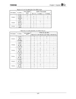
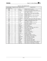
3.1.14 Extended EJTAG Interface Signals
Table 3.1.14 Extended EJTAG Interface Signals (1/2)
Signal Name
Type
Description
Initial State
TCK Input
PU
JTAG Test Clock Input
Clock input signal for JTAG.
TCK is used to execute JTAG instructions and input/output data.
Input
TDI/DINT
*
Input
PU
JTAG Test Data Input/Debug Interrupt
When PC trace mode is not selected, this signal is a JTAG data input signal. It is used
to input serial data to JTAG data/instruction registers.
When PC trace mode is selected, this signal is an interrupt input signal used to cancel
PC trace mode for the debug unit.
Input
TDO/TPC[0]
Output
JTAG Test Data Output/PC Trace Output
When PC trace mode is not selected, this signal is a JTAG data output signal. Data is
output by means of serial scan.
When PC trace mode is selected, this signal outputs the value of the noncontiguous
program counter in sync with the debug clock (DCLK).
Input
Содержание TMPR4925
Страница 1: ...64 Bit TX System RISC TX49 Family TMPR4925 Rev 3 0 ...
Страница 4: ......
Страница 15: ...Handling Precautions ...
Страница 16: ......
Страница 18: ...1 Using Toshiba Semiconductors Safely 1 2 ...
Страница 40: ...3 General Safety Precautions and Usage Considerations 3 18 ...
Страница 42: ...4 Precautions and Usage Considerations 4 2 ...
Страница 43: ...TMPR4925 ...
Страница 44: ......
Страница 54: ...Chapter 1 Features 1 8 ...
Страница 58: ...Chapter 2 Block Diagram 2 4 ...
Страница 88: ...Chapter 4 Address Mapping 4 12 ...
Страница 226: ...Chapter 8 DMA Controller 8 58 ...
Страница 260: ...Chapter 9 SDRAM Controller 9 34 ...
Страница 480: ...Chapter 15 Interrupt Controller 15 32 ...
Страница 554: ...Chapter 19 Real Time Clock RTC 19 8 ...
Страница 555: ...Chapter 20 Removed 20 1 20 Removed ...
Страница 556: ...Chapter 20 Removed 20 2 ...
Страница 564: ...Chapter 21 Extended EJTAG Interface 21 8 ...
Страница 580: ...Chapter 22 Electrical Characteristics 22 16 ...
Страница 586: ...Chapter 23 Pin Layout Package 23 6 23 2 Package Package Type Package Code 256 pin PBGA PBGA 4L P BGA256 2727 1 27A4 ...
Страница 588: ...Chapter 24 Usage Notes 24 2 ...
Страница 590: ...Appendix A TX49 H2 Core Supplement A 2 ...


