Chapter 16 CHI Module
16-5
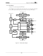
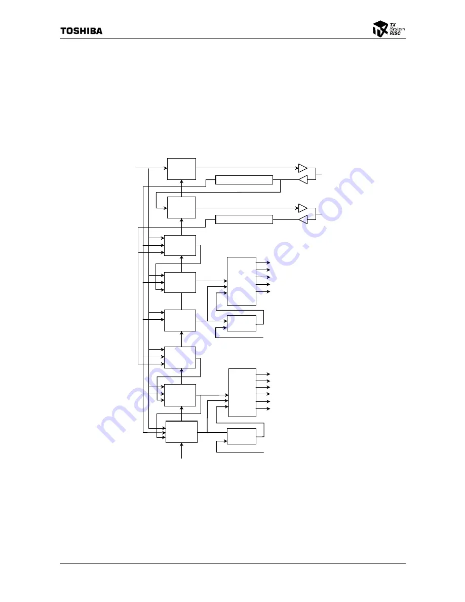
The programmable receive channel counter output is constantly compared with the receive TDM
switch control register values, and whenever a match occurs, the byte of data is loaded from the receive
shift register into the correct field within the receive holding register. Similarly, the programmable
transmit channel counter output is constantly compared with the transmit TDM switch control register
values, and whenever a match occurs, the byte of data is loaded from the correct field within the
transmit holding register into the receive shift register.
All control registers, including the TDM switch control registers, must be unchanged while the CHI
Module is enabled. If any register is changed during the CHI operation, the result is undefined.
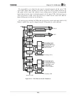
Figure 16.3.2 CHI Clock and Control Generation
PRGM TX
FS Delay
CNT
PRGM
RX CHAN
CNT
÷
8/16
RX Bit
CNT
PRGM RX
FS Delay
CNT
PRGM
CHIFS
Divider
PRGM
CHICLK
Divider
CMP
Decode
RX Start/Stop Control
RX Shift REG Control
RX Holding REG Control
RX DMA REQ Control
Sample Interrupt
RX TDM Switch CNTL
CHIFS
IMBUSCLK
CHICLK
SYNCH Digital PLL
SYNCH Digital PLL
PRGM
TX CHAN
CNT
÷
8/16
TX Bit
CNT
Control from CPU
Decode
TX Start/Stop Control
TX Shift REG Control
TX Holding REG Control
TX DMA REQ Control
Sample Interrupt
TX CHIDOUT Enable
TX TDM Switch CNTL
CMP
Содержание TMPR4925
Страница 1: ...64 Bit TX System RISC TX49 Family TMPR4925 Rev 3 0 ...
Страница 4: ......
Страница 15: ...Handling Precautions ...
Страница 16: ......
Страница 18: ...1 Using Toshiba Semiconductors Safely 1 2 ...
Страница 40: ...3 General Safety Precautions and Usage Considerations 3 18 ...
Страница 42: ...4 Precautions and Usage Considerations 4 2 ...
Страница 43: ...TMPR4925 ...
Страница 44: ......
Страница 54: ...Chapter 1 Features 1 8 ...
Страница 58: ...Chapter 2 Block Diagram 2 4 ...
Страница 88: ...Chapter 4 Address Mapping 4 12 ...
Страница 226: ...Chapter 8 DMA Controller 8 58 ...
Страница 260: ...Chapter 9 SDRAM Controller 9 34 ...
Страница 480: ...Chapter 15 Interrupt Controller 15 32 ...
Страница 554: ...Chapter 19 Real Time Clock RTC 19 8 ...
Страница 555: ...Chapter 20 Removed 20 1 20 Removed ...
Страница 556: ...Chapter 20 Removed 20 2 ...
Страница 564: ...Chapter 21 Extended EJTAG Interface 21 8 ...
Страница 580: ...Chapter 22 Electrical Characteristics 22 16 ...
Страница 586: ...Chapter 23 Pin Layout Package 23 6 23 2 Package Package Type Package Code 256 pin PBGA PBGA 4L P BGA256 2727 1 27A4 ...
Страница 588: ...Chapter 24 Usage Notes 24 2 ...
Страница 590: ...Appendix A TX49 H2 Core Supplement A 2 ...


