


MAX32600 User’s Guide
System Configuration and Management
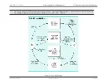
4.1 Power Ecosystem and Operating Modes
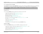
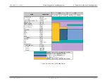
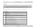
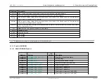
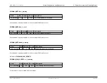
Pin Name
Description
V
DDA3DAC
DAC / op amp power input (3V nominal). Connect to V
DDA3
directly or via a filter network.
V
DDA3REF
Reference power input (3V nominal). Connect to V
DDA3
directly or via a filter network.
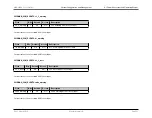
V
REFADC
ADC reference voltage output. Buffered output can be set to 1.024V, 1.5V, 2.048V, and 2.5V. This pin must be
connected to V
SS
through a 4.7uF capacitor.
V
REFDAC
DAC reference voltage output. Buffered output can be set to 1.024V, 1.5V, 2.048V, and 2.5V. This pin must be
connected to V
SS
through a 4.7uF capacitor.
V
REFADJ
Precision reference input that may be optionally used be in place of internal reference by V
REFADC
and V
REFDAC
buffers. Ground if not used.
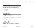
V
SS
Digital Ground. Tie all grounds together on circuit board.
V
SSUB
Substrate Ground.
V
SSREF
Reference Ground.
V
SSADC
ADC Ground.
V
SSDAC
DAC Ground.
Note
All grounds are assumed to be tied together at the circuit board level.
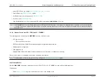
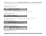
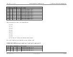
4.1.12
Registers (PWRMAN)
4.1.12.1
Module PWRMAN Registers
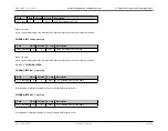
Address
Register
32b
Word Len
Description
0x40090800
1
Power Reset Control and Status
0x40090804
1
Interrupt Flags
0x40090808
1
Interrupt Enable/Disable Controls
0x4009080C
1
SVM Event Status Flags (read-only)
0x40090810
1
Wake-Up Detect Control
0x40090814
1
WUD Pulse To Mode Bit 0
0x40090818
1
WUD Pulse To Mode Bit 1
0x40090830
1
Wake-up Detect Status for P0/P1/P2/P3
0x40090834
1
Wake-up Detect Status for P4/P5/P6/P7
Rev.1.3 April 2015
Maxim Integrated
Page 43
Содержание MAX32600
Страница 1: ...MAX32600 User s Guide April 2015...


