MAX32600 User’s Guide
System Configuration and Management
4.1 Power Ecosystem and Operating Modes
4.1.10
Reset Pins
The
MAX32600
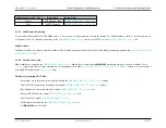
contains two active low reset pins, RSTN and SRTSN. RSTN serves as the main chip reset input. Asserting the pin low will reset all registers on the
chip except RTC related circuits and wakeup configuration. This allows a restart of all chip functions (analog and digital) while still maintaining the Real Time Clock.
Note
Asserting RSTN will turn off the 1.8V LDO but external capacitance will keep the V
REG18
rail and SRAM data intact during a momentary reset pulse.
A continued RSTN assertion will keep the 1.8V LDO off, eventually causing the V
REG18
rail to collapse and lose all SRAM data.
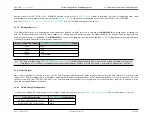
SRSTN is a bidirectional reset that will perform a reset to the digital core when asserted low and will subsequently drive a reset pulse to other components in the
system.
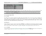
To fully reset the entire chip including RTC related circuitry, all three main power inputs (V
BUS
, V
DD
, V
RTC
) must be powered down.
4.1.11
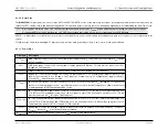
Power Pins
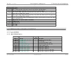
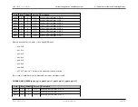
Pin Name
Description
V
DD
Main chip power input. Connect to 3V nominal power supply or battery. This pin must be connected to V
SS
through
a 4.7uF capacitor.
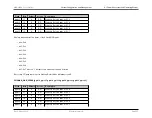
V
BUS
USB power input. Connect a 5V nominal power supply, typically USB power. This pin must be connected to V
SS
through a 4.7uF capacitor.
V
DDB
Output of USB 5V -
>
3.3V LDO. This pin must be connected to V
SS
through a 4.7uF capacitor
V
RTC
Backup rail or “Last Man Standing” rail. Connect to super capacitor or 3V nominal power supply or battery. This
pin must be connected to V
SS
through a 1.0uF capacitor if connected to a 3V nominal power supply or battery.
Connect to V
DD
if backup rail is not used.
V
DDIO
3V nominal GPIO power. This pin (connected to Ports 6, 7) must be connected to V
SS
through a 4.7uF capacitor (if
the 12mm x 12mm package is used). Up to 50mA may be sourced for external components.
Note: On the 12mm
x 12mm package, all GPIOs are powered by V
VDDIO
.
V
DDIO_SW1
3V / 1.8V nominal GPIO power. Bank of GPIOs (connected to Ports 0, 1 on the 12mm x 12mm package and Port
1 on the 7mm x 7mm package) using V
DDIO
(3V nominal) or V
REG18
(1.8V nominal) as a power source. This pin
must be connected to V
SS
through a 1.0uF capacitor.
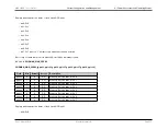
V
DDIO_SW2
3V / 1.8V nominal GPIO power. Bank of GPIOs (connected to Ports 2, 3, 4, 5 on the 12mm x 12mm package, Port
2 on the 7mm x 7mm package, and JTAG) using V
DDIO
(3V nominal) or V
REG18
(1.8V nominal) as a power source.
This pin must be connected to V
SS
through a 1.0uF capacitor.
V
DDA3
Analog power source (3V nominal). Option to connect filter network between V
DDA3
and V
DDA3ADC
/ V
DDA3DAC
/
V
DDA3REF
. Short to V
DDA3
pins if filter network not needed.
V
DDA3ADC
ADC power input (3V nominal). Connect to V
DDA3
directly or via a filter network.
Rev.1.3 April 2015
Maxim Integrated
Page 42
Содержание MAX32600
Страница 1: ...MAX32600 User s Guide April 2015...


