MAX32600 User’s Guide
Communication Peripherals
7.2 SPI
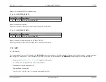
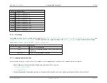
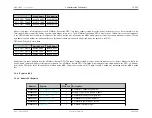
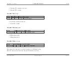
Start Address
End Address
SPI0_FIFO_TRANS
0x4010_0000
0x4010_07FE
SPI1_FIFO_TRANS
0x4010_1000
0x4010_17FE
SPI2_FIFO_TRANS
0x4010_2000
0x4010_27FE
Writes to this space result in pushes to the SPI Master Transaction FIFO. This space supports single accesses as well as burst accesses. Access widths of 8-bit,
16-bit, and 32-bit are supported. Reads from this space always return zeros. The SPI Master Transaction FIFO is 2-bytes wide. 16-bit writes result in a single push
to the FIFO. 32-bit writes result in two FIFO pushes, the LSW is pushed first, followed by the MSW. 8-bit writes must occur in even/odd byte address pairs. The odd
byte address data is held by the slave until the even byte address data is written, at which point 2-bytes are pushed to the FIFO.
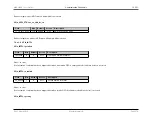
FIFO Read Points for Results Data
Start Address
End Address
SPI0_FIFO_RSLTS
0x4010_0800
0x4010_0FFF
SPI1_FIFO_RSLTS
0x4010_1800
0x4010_1FFF
SPI2_FIFO_RSLTS
0x4010_2800
0x4010_2FFF
Reads from this space pull data from the SPI Master Results FIFO. This space supports single accesses as well as burst accesses. Access widths of 8-bit, 16-bit,
and 32-bit are supported. Writes to this space are ignored. The SPI Master Results FIFO is 1-bit wide. 8-bit reads result in a single pull from the FIFO. 16- bit reads
result in two FIFO pulls, the LSB is pulled first, followed by the MSB. 32-bit reads result in four FIFO pulls, the LSB is pulled first, continuing until the MSB is pulled
last.
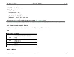
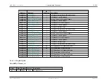
7.2.9
Registers (SPI)
7.2.9.1
Module SPI Registers
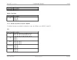
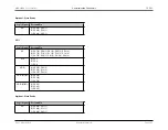
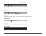
Address
Register
32b
Word Len
Description
0x40030000
1
SPI Master Configuration Register
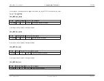
0x40030004
1
Polarity Control for SS and SR Signals
0x40030008
1
SPI Master General Control Register
0x4003000C
1
SPI Master FIFO Control Register
0x40030010
1
SPI Master Special Mode Controls
0x40030014
1
SPI Master Interrupt Flags
Rev.1.3 April 2015
Maxim Integrated
Page 269
Содержание MAX32600
Страница 1: ...MAX32600 User s Guide April 2015...


