


MAX32600 User’s Guide
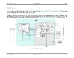
Analog Front End
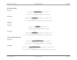
8.3 ADC
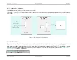
ADC+
ADC-
Notes
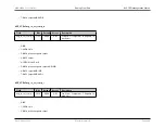
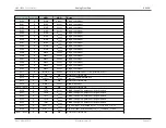
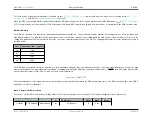
0x31
X
V
REFDAC
V
AGND
V
REFDAC
output buffer
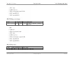
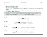
0x32
X
V
REFADC
V
AGND
V
REFDAC
output buffer
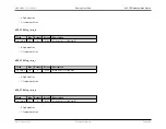
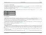
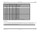
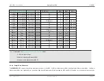
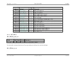
0x00
1
AIN0
AIN8
Differential Input
0x01
1
AIN1
AIN9
Use differential AIN1/9 for external V
BE
-Resistor temperature sen-
sor
0x02
1
AIN2
AIN10
Differential Input
0x03
1
AIN3
AIN11
Differential Input
0x04
1
AIN4
AIN12
Differential Input
0x05
1
AIN5
AIN13
Differential Input
0x06
1
AIN6
AIN14
Differential Input
0x07
1
AIN7
AIN15
Differential Input
0x08
1
AIN0
AIN8
Differential Input
0x09
1
AIN1
AIN9
Differential Input
0x0A
1
AIN2
AIN10
Differential Input
0x0B
1
AIN3
AIN11
Differential Input
0x0C
1
AIN4
AIN12
Differential Input
0x0D
1
AIN5
AIN13
Differential Input
0x0E
1
AIN6
AIN14
Differential Input
0x0F
1
AIN7
AIN15
Differential Input
0x11
1
TMON_R
TMON_VBE
V
BE
measurement for Temperature Sensor
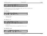
Advanced Details
Input Mux Leakage Current
: The input mux is structured to minimize the input leakage, typically as low as a few pA. The input switch chosen by
is only closed for the duration of the ADC/PGA acquisition window window (nominally 187.5ns and 1.75us, respectively). During this acquisition
period, a large current will flow into the ADC/PGA capacitors. As the capacitive charge settles, the current will return to the original low-leakage value.
Note
The longer PGA acquisition time can be useful for weaker inputs.
Rev.1.3 April 2015
Maxim Integrated
Page 412
Содержание MAX32600
Страница 1: ...MAX32600 User s Guide April 2015...


