MAX32600 User’s Guide
Communication Peripherals
7.2 SPI
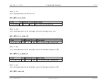
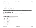
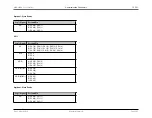
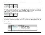
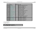
SPI2
Logic Signal
Port and Pin
SS
A/B) P2.3(0), P1.4(1), P1.5(2), P1.6(3) P1.7(4)
SCK
A/B) P2.0
SDIO
A/B) P1.6(2), P1.7(3)
SDIO (MOSI)
A/B) P2.1(0)
SDIO (MISO)
A/B) P2.2(1)
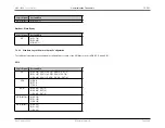
Optional: Slave Ready
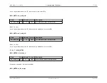
Logic Signal
Port and Pin
SR
A) P2.7(0)
B) P1.4(0)
A/B) P1.5(1)
7.2.3
Clock Selection and Configuration
The
MAX32600
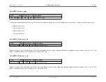
supports programmable SPI clock rates, which are a divisor of the system clock. Each of the three SPI ports is able to set its clock rate independently.
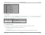
To set the base clock rate, write to the appropriate Clock Control register with the value desired to achieve the ideal clock rate for the slave devices.
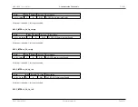
SPI Clock Control Registers
Port
SPI Clock Control Register
SPI0
SPI1
SPI2
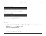
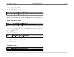
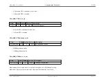
Setting the SPI Clock Rate -
CLKMAN_CLK_CTRL_[N]_SPI[x]
[3:0]
SPI Clock Rate
0000b
Disabled
0001b
(System Clock Source / 1)
Rev.1.3 April 2015
Maxim Integrated
Page 262
Содержание MAX32600
Страница 1: ...MAX32600 User s Guide April 2015...

