


MAX32600 User’s Guide
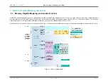
Memory, Register Mapping, and Access
3.2 Standard Memory Regions
Note
The ARM Cortex-M3 core translates the access in the bit-banding alias area into the appropriate read cycle (for a single bit read) or a read-modify-
write cycle (for a single bit set or clear) of the bit-banding primary area. This means that bit-banding is a core function (i.e., not a function of the SRAM
memory interface layer or the AHB bus layer), and thus is only applicable to accesses generated by the core itself. Reads/writes to the bit-banding
alias area by other (non-ARM-core) bus masters such as the PMU AHB bus master will not trigger a bit-banding operation and will instead result in
an AHB bus error.
The SRAM area on the
MAX32600
can be used to contain executable code. Code stored in the SRAM is accessed directly for execution (using the system bus) and
is not cached or code scrambled.
The SRAM is also where the ARM Cortex-M3 stack must be located, as it is the only general-purpose SRAM memory on the device. A valid stack location inside the
SRAM must be set by the system exception table stored in the main program flash.
The general purpose PMU engine and the function specific AHB bus master included in the USB peripheral block can both access the SRAM to use as general
storage or working space. Specifically in the case of the USB interface, SRAM memory area can be used to store the descriptor table for the endpoint buffers as well
as the endpoint buffers themselves.
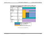
3.2.3
Peripheral Space
The peripheral space area of memory is intended for mapping of control registers, internal buffers/working space, and other features needed for the firmware control
of non-core peripherals. It is defined from byte address range 0x4000_0000 to 0x5FFF_FFFF (0.5GB maximum). On the
MAX32600
, this includes such functions
as the
, etc.),
interfaces,
, etc.
As with the SRAM region, there is a dedicated 1MB area at the bottom of this memory region (from 0x4000_0000 to 0x400F_FFFF) that is used for bit-banding
operations by the ARM core. Read/write operations in the peripheral bit-banding alias area (32MB in length, from 0x4200_0000 to 0x43FF_FFFF) are translated by
the core into read/mask/shift or read/modify/write operation sequences to the appropriate location in the bit-banding area.
Note
The bit-banding operation within peripheral memory space is, like bit-banding function in SRAM space, a core remapping function, and it is only
applicable to operations performed directly by the ARM core. If another memory bus master accesses the peripheral bit-banding region (e.g., the
JTAG/PTP AHB master or the PMU AHB master), the bit-banding operation will not take place, and the bit-banding alias region will appear to be a
non-implemented memory area (causing an AHB bus error).
On the
MAX32600
, access to the region that contains most peripheral registers (0x4000_0000 to 0x400F_FFFF) goes from the AHB bus through an AHB-to-APB
bridge. This allows the peripheral blocks to operate on the slower, easier to handle APB bus matrix while also ensuring that peripherals with slower response times
do not tie up bandwidth on the AHB bus, which must necessarily have a faster response time since it handles main application instruction and data fetching.
A secondary region within the peripheral memory space is set aside for other peripherals that require more rapid data transfer to implement direct access AHB
slave instances (0x04010_0000 to 0x401F_FFFF). This area is used so that peripherals which have FIFOs or other functions requiring large amounts of data to be
transferred quickly (such as the ADC and DACs) can benefit from the more rapid transfers available on the AHB bus.
Rev.1.3 April 2015
Maxim Integrated
Page 25
Содержание MAX32600
Страница 1: ...MAX32600 User s Guide April 2015...


