


MAX32600 User’s Guide
Communication Peripherals
7.2 SPI
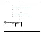
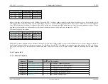
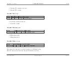
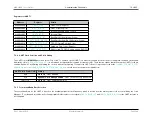
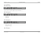
SPIn_GEN_CTRL.bb_sr_in
Field
Bits
Default
Access
Description
bb_sr_in
5
0
R/O
Bit Bang SR Input
Writes have no effect.
When read, returns the current state of the flow control (0=deasserted, 1=asserted)
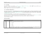
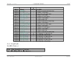
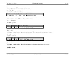
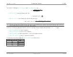
SPIn_GEN_CTRL.bb_sck_in_out
Field
Bits
Default
Access
Description
bb_sck_in_out
6
0
R/W
Bit Bang SCK Input/Output
When written, defines output state of SPI clock signal SCK (Bit Bang Mode only)
When read, returns the current state of the SCK clock (0=inactive, 1=active)
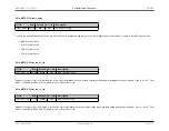
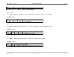
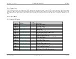
SPIn_GEN_CTRL.bb_sdio_in
Field
Bits
Default
Access
Description
bb_sdio_in
11:8
0000b
R/O
Bit Bang SDIO Input
Writes have no effect.
When read, returns the current input state of the SDIO pins
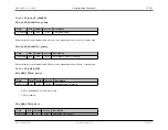
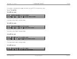
SPIn_GEN_CTRL.bb_sdio_out
Field
Bits
Default
Access
Description
bb_sdio_out
15:12
0000b
R/W
Bit Bang SDIO Output
Rev.1.3 April 2015
Maxim Integrated
Page 276
Содержание MAX32600
Страница 1: ...MAX32600 User s Guide April 2015...


