MAX32600 User’s Guide
Pin Configurations, Packages, and Special Function Multiplexing
5.3 General-Purpose I/O
5.3
General-Purpose I/O
The
MAX32600
includes 64 general-purpose I/O (GPIO) pins which can be controlled directly by firmware or indirectly by other hardware functions (such as output
peripherals). GPIOs can be powered by either V
DDIO
or V
REG18
(reference
for detailed information).
These GPIO pins are logically divided into eight GPIO ports, each port consisting of eight pins. The ports are named as follows: P0, P1, P2, P3, P4, P5, P6, and P7.
A single GPIO pin within a port is typically referred to by the notation (port).(pin), where the pin within each port is numbered from 0 to 7. For example, the third pin
in Port 2 is referred to as P2.2.
Features supported by the GPIO module include the following:
• Functions are selectable on a per-pin basis, with GPIO operation (meaning that the firmware controls the state of the pin) being the lowest-priority function
type.
• When a pin is using GPIO functionality, firmware can directly control the drive strength and output type of the pin (e.g., normal drive vs. open-drain or
high-impedance).
• Regardless of the selected function for a given pin, firmware can always monitor the current logic level of the pin using the appropriate registers.
–
All GPIO pins support interrupt detection based on input signals external to the device.
–
Interrupts may be detected on rising or falling edges or high/low levels.
–
Interrupts to the CPU are generated on a per-port basis; i.e., any interrupts originating from Port 0 are assigned to a single interrupt vector, interrupts
from Port 1 are assigned to a different vector, and so on.
• When in GPIO operation, simple output-only functions can be assigned to a GPIO pin:
–
Output from Pulse Trains (0 through 7)
–
Output from Timers running in 32-bit mode
–
In this case, output drive strength and type will still be determined by firmware
Memory Mapping
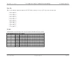
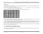
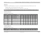
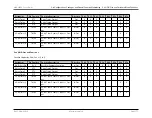
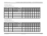
The GPIO module is controlled and configured by a set of registers mapped into data memory space as follows.
• Access through AHB System Bus to peripheral space (0x4000_0000..0x5FFF_FFFF)
–
AHB-to-APB Bridge (0x4000_0000..0x400F_FFFF)
* GPIO APB Bus Slave (0x4000_0000..0x4000_0FFF)
The GPIO module does not include any registers or data areas mapped into AHB peripheral space (from 0x4010_0000..0x401F_FFFF).
Rev.1.3 April 2015
Maxim Integrated
Page 173
Содержание MAX32600
Страница 1: ...MAX32600 User s Guide April 2015...


