239
────────────────────────────────────────────────────
14.4 Internal Block Diagram
────────────────────────────────────────────────────
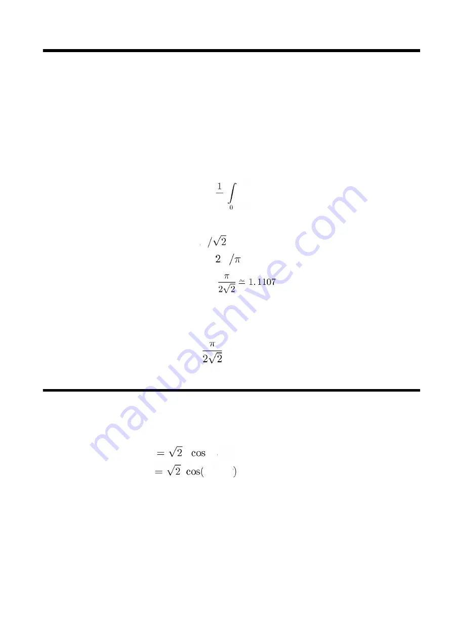
14.4.2 MEAN Value (MEAN rectification effective value for
display)
Averaging value =
|e|dt
T
T
e
RMS value =
Averaging value =
RMS value
─────── =
Averaging value
A
A
MEAN value =
×
Averaging value
14.4.3 Active Power
E
RMS value of voltage
I
RMS value of current
ω
angular frequency
t
time
θ
phase difference between voltage
waveform and current waveform
+
e
i
E
ω
t
I
ω
t
θ
For MEAN values, the input signal waveform is converted to a DC voltage
by an absolute value detecting circuit and a smoothing circuit Since this is
an analog process, all signals within the frequency range of the specification
are converted precisely.
This is found using an absolute value detecting circuit and a smoothing
circuit. The theoretical expression used here for the MEAN value is as
follows:
However, using this expression as it is for a sine wave of amplitude
A
and
period 2
π
, results in RMS and average values as follows:
And thus for the same measured sine wave the figures do not agree. For this
reason, to make the figures agree when a sine wave signal is input, the
average value defined above is multiplied by a coefficient to give the MEAN
value (mean rectification effective value for display).
If the sine wave voltage and sine wave current are e and i respectively, then
this can be expressed as follows:
The instantaneous power
p
is the product of
e
and
i
, as follows:
p
=
e
・
i
= 2
EI
cos
ω
t
・
cos (
ω
t
+
θ
)
=
EI
cos(2
ω
t
+
θ
)+
EI
cos
θ
The DC component in this expression is the active power
P
:
P
=
EI
cos
θ
In the internal circuit, the instantaneous power
p
is computed by a multiplier
IC, and the active power
P
is obtained by smoothing to give a DC voltage
proportional to the active power
P
.
Summary of Contents for Power HiTester 3193
Page 2: ......
Page 50: ...32 3 9 Operations During Power Failure ...
Page 76: ...58 4 13 Degaussing ...
Page 80: ...62 5 2 Setting the Frequency Range fa ...
Page 108: ...90 9 3 Internal Circuit for the External Control and Timing ...
Page 112: ...94 10 3 Output Rate ...
Page 250: ...232 13 9 Error and Overflow Displays ...
Page 278: ...260 17 5 Internal Block Diagram ...
Page 284: ...266 19 2 Installation Procedures For JIS standard For EIA standard External Dimensions ...
Page 300: ...282 20 4 Internal Block Diagram of the 3193 ...
Page 306: ...INDEX 4 Index ...
Page 307: ......
Page 308: ......
Page 309: ......
Page 310: ......


