407
•
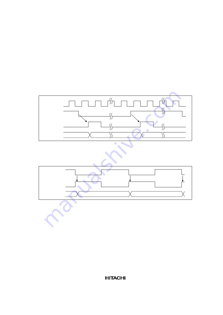
External Clock Operation: Set the TPSC2–TPSC0 bits in TCR to select the external clock
(TCLK) as the timer clock. Use the CKEG1 and CKEG0 bits in TCR to select the detection
edge. Rising, falling, or both edges may be selected. The pulse width of the external clock
must be at least 1.5 peripheral module clock cycles for single edges or 2.5 peripheral module
clock cycles for both edges. A shorter pulse width will result in accurate operation. Figure 12.5
shows the timing for both-edge detection.
P
φ
External
clock input
pin (TCLK)
TCNT
input clock
TCNT
N + 1
N
N – 1
Figure 12.5 Count Timing when Operating on External Clock (Both Edges Detected)
•
On-Chip RTC Clock Operation: Set the TPSC2–TPSC0 bits in TCR to select the on-chip RTC
clock as the timer clock. Figure 12.6 shows the timing.
RTC output
clock
TCNT
TCNT input
clock
N + 1
N
N – 1
Figure 12.6 Count Timing when Operating on On-Chip RTC Clock
12.3.2
Input Capture Function
Channel 2 has an input capture function (figure 12.7). When using the input capture function, set
the TCLK pin to input mode with the TCOE bit in the timer output control register (TOCR) and
set the timer operation clock to internal clock or on-chip RTC clock with the TPCS2–TPCS0 bits
in the timer control register (TCR2). Also, designate use of the input capture function and whether
to generate interrupts on input capture with the IPCE1–IPCE0 bits in TCR2, and designate the use
of either the rising or falling edge of the TCLK pin to set the timer counter (TCNT2) value into the
input capture register (TCPR2) with the CKEG1–CKEG0 bits in TCR2.
The input capture function cannot be used in standby mode.
Содержание SH7709S
Страница 2: ...Hitachi SuperH RISC engine SH7709S Hardware Manual ADE 602 250 Rev 1 0 09 21 01 Hitachi Ltd ...
Страница 75: ...56 ...
Страница 107: ...88 ...
Страница 125: ...106 ...
Страница 139: ...120 ...
Страница 203: ...184 ...
Страница 245: ...226 ...
Страница 292: ...273 T1 CKIO A25 to A0 CSn RD WR RD D31 to D0 WEn D31 to D0 BS T2 Read Write Figure 10 6 Basic Timing of Basic Interface ...
Страница 323: ...304 Tp TRr TRrw TRrw CKIO CKE CSn RAS3U RAS3L CASU CASL RD WR Figure 10 28 Synchronous DRAM Auto Refresh Timing ...
Страница 411: ...392 ...
Страница 609: ...590 ...
Страница 635: ...616 ...
Страница 663: ...644 ...
Страница 679: ...660 ...


