643
21.3
Operation
The D/A converter has two built-in D/A conversion circuits that can perform conversion
independently.
D/A conversion is performed constantly while enabled in DACR. If the DADR0 or DADR1 value
is modified, conversion of the new data begins immediately. The conversion results are output
when bits DAOE0 and DAOE1 are set to 1.
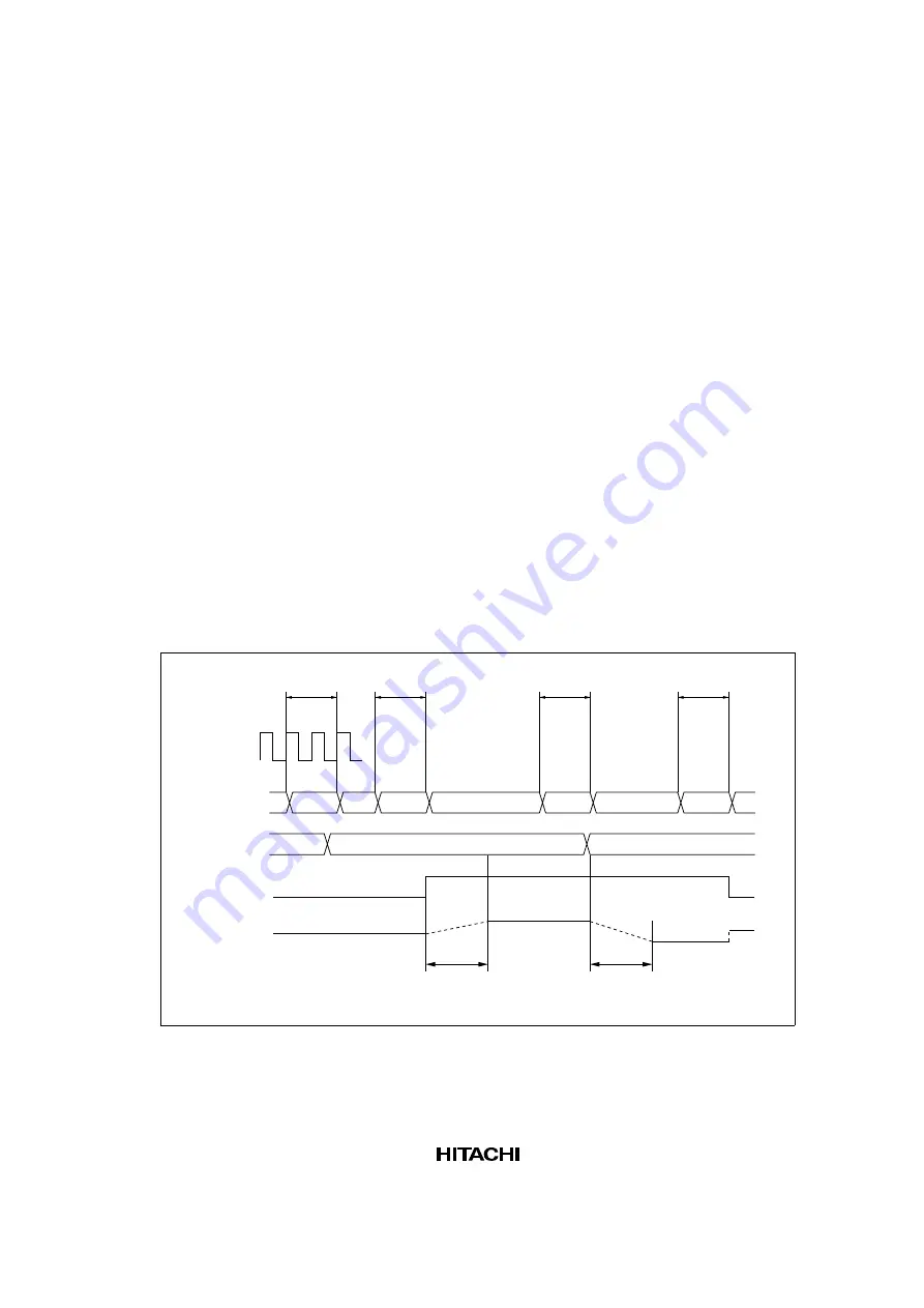
An example of D/A conversion on channel 0 is given next. Timing is indicated in figure 21.2.
1. Data to be converted is written in DADR0.
2. Bit DAOE0 is set to 1 in DACR. D/A conversion starts and DA0 becomes an output pin. The
converted result is output after the conversion time. The output value is (DADR0 contents/256)
×
AVcc. Output of this conversion result continues until the value in DADR0 is modified or
the DAOE0 bit is cleared to 0.
3. If the DADR0 value is modified, conversion starts immediately, and the result is output after
the conversion time.
4. When the DAOE0 bit is cleared to 0, DA0 becomes an input pin.
DADR0
write cycle
t
DCONV
High-impedance state
Conversion
result 1
Conversion data 1
Conversion data 2
Conversion
result 2
t
DCONV
ø
Address bus
DADR0
DAOE0
DA0
t
DCONV
: D/A conversion time
Legend
DACR
write cycle
DADR0
write cycle
DACR
write cycle
Figure 21.2 Example of D/A Converter Operation
Содержание SH7709S
Страница 2: ...Hitachi SuperH RISC engine SH7709S Hardware Manual ADE 602 250 Rev 1 0 09 21 01 Hitachi Ltd ...
Страница 75: ...56 ...
Страница 107: ...88 ...
Страница 125: ...106 ...
Страница 139: ...120 ...
Страница 203: ...184 ...
Страница 245: ...226 ...
Страница 292: ...273 T1 CKIO A25 to A0 CSn RD WR RD D31 to D0 WEn D31 to D0 BS T2 Read Write Figure 10 6 Basic Timing of Basic Interface ...
Страница 323: ...304 Tp TRr TRrw TRrw CKIO CKE CSn RAS3U RAS3L CASU CASL RD WR Figure 10 28 Synchronous DRAM Auto Refresh Timing ...
Страница 411: ...392 ...
Страница 609: ...590 ...
Страница 635: ...616 ...
Страница 663: ...644 ...
Страница 679: ...660 ...


