272
DREQ
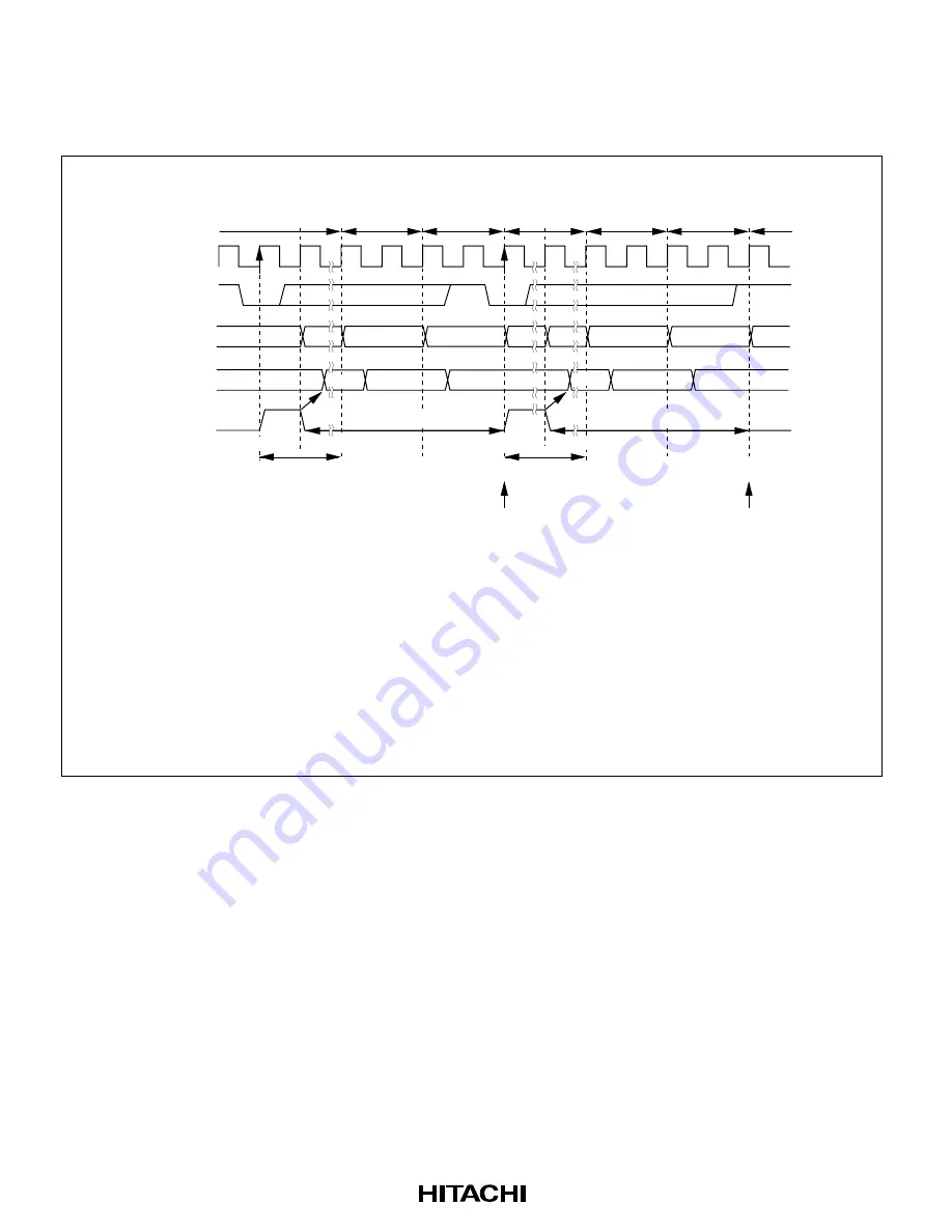
Pin Falling Edge Activation Timing: Set the DTA bit for the channel for which the
DREQ
pin is selected to 1.
Figure 8-23 shows an example of
DREQ
pin falling edge activated normal mode transfer.
[1]
[2] [5]
[3] [6]
[4] [7]
Note: In write data buffer mode, bus breaks from [2] to [7] may be hidden, and not visible.
Acceptance after transfer enabling; the
DREQ
pin low level is sampled on the rising
edge of ø, and the request is held.
The request is cleared at the next bus break, and activation is started in the DMAC.
Start of DMA cycle;
DREQ
pin high level sampling on the rising edge of ø starts.
When the
DREQ
pin high level has been sampled, acceptance is resumed after the
write cycle is completed.
(As in [1], the
DREQ
pin low level is sampled on the rising edge of ø, and the request
is held.)
DMA
read
ø
Address bus
DREQ
Idle
Write
Idle
Bus release
DMA control
Channel
Write
Idle
Transfer
source
Request
Minimum of 2 cycles
[1]
[3]
[2]
[4]
[6]
[5]
[7]
Acceptance resumes
Acceptance resumes
DMA
write
Bus
release
DMA
read
DMA
write
Bus
release
Request
Minimum of 2 cycles
Transfer
destination
Transfer
source
Transfer
destination
Request clear period
Request clear period
Read
Read
Figure 8-23 Example of
DREQ
Pin Falling Edge Activated Normal Mode Transfer
DREQ
pin sampling is performed every cycle, with the rising edge of the next ø cycle after the
end of the DMABCR write cycle for setting the transfer enabled state as the starting point.
When the
DREQ
pin low level is sampled while acceptance by means of the
DREQ
pin is
possible, the request is held in the DMAC. Then, when activation is initiated in the DMAC, the
request is cleared, and
DREQ
pin high level sampling for edge detection is started. If
DREQ
pin
high level sampling has been completed by the time the DMA write cycle ends, acceptance
resumes after the end of the write cycle,
DREQ
pin low level sampling is performed again, and
this operation is repeated until the transfer ends.
Содержание H8S/2631
Страница 28: ...xviii Appendix G Package Dimensions 1154 ...
Страница 341: ...316 Transfer SAR or DAR DAR or SAR Block area First block Nth block Figure 9 8 Memory Mapping in Block Transfer Mode ...
Страница 918: ...905 ø DREQ0 DREQ1 tDRQS tDRQH Figure 25 19 DMAC DREQ Input Timing ...
Страница 955: ...943 A 2 Instruction Codes Table A 2 shows the instruction codes ...


