


ESD Protection
R
100
»
W
ADC14MCTLx.0–4
Input
Ax
Precision ADC Operation
846
SLAU356I – March 2015 – Revised June 2019
Copyright © 2015–2019, Texas Instruments Incorporated
Precision ADC
22.2.2 Precision ADC Inputs and Multiplexer
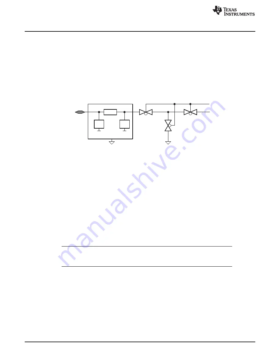
Up to 32 external and up to 6 internal analog signals are available, and the channel for conversion is
selected by the analog input multiplexer. The number of channels available is device specific and given in
the device-specific data sheet. The input multiplexer is a break-before-make type to reduce input-to-input
noise injection resulting from channel switching (see
). The input multiplexer is also a T-switch
to minimize the coupling between channels. Channels that are not selected are isolated from the A/D and
the intermediate node is connected to analog ground (AV
SS
), so that the stray capacitance is grounded to
eliminate crosstalk.
The Precision ADC uses the charge redistribution method. When the inputs are internally switched, the
switching action may cause transients on the input signal. These transients decay and settle before
causing errant conversion.
Figure 22-2. Analog Multiplexer
22.2.2.1 Analog Port Selection
The Precision ADC inputs are multiplexed with digital port pins. When analog signals are applied to digital
gates, parasitic current can flow from V
CC
to GND. This parasitic current occurs if the input voltage is near
the transition level of the gate. Disabling the digital part of the port pin eliminates the parasitic current flow
and reduces overall current consumption. The PySELx bits provide the ability to disable the port pin input
and output buffers.
22.2.3 Voltage References
The Precision ADC module may use an on-chip shared reference module that supplies three selectable
voltage levels of 1.2 V, 1.45 V, and 2.5 V (see the REF module chapter for configuration details) to supply
V
R+
and V
R–
. These reference voltages may be used internally and externally on pin VREF+. Alternatively,
external references may be supplied for V
R+
and V
R–
through pins VREF+/VeREF+ and VeREF-,
respectively. TI recommends connecting VeREF- to onboard ground when using ADC14VRSEL settings
1110b or 1111b.
NOTE:
The maximum sampling rate of Precision ADC is limited to 200 ksps when the internal
reference is used together with BUF_EXT (ADC14VRSEL = 0001b and REFOUT = 1). In all
other reference settings the Precision ADC sampling rate can be up to 1 Msps.
22.2.4 Auto Power Down
The Precision ADC is designed for low-power applications. When the Precision ADC is not actively
converting, the core is automatically disabled and automatically reenabled when needed. The MODOSC
or SYSOSC are also automatically enabled to provide MODCLK or SYSCLK to Precision ADC when
needed and disabled when not needed for Precision ADC or for rest of the device.
22.2.5 Power Modes
The Precision ADC supports two power modes selected through the ADC14PWRMD bits in the
ADC14CTL1 register. ADC14PWRMD = 00b selects regular-power mode, and ADC14PWRMD = 10b
selects low-power mode. Precision ADC supports 8-, 10-, 12-, and 14-bit resolution settings selected
through the ADC14RES bits in the ADC14CTL1 register.


