background image

If the objective of synchronization is to achieve a relative time within the substation and if no

station master clock with minute pulse output is available, a simple minute pulse generator can be

designed and used for synchronization of the IEDs. The minute pulse generator can be created

using the logical elements and timers available in the IED.

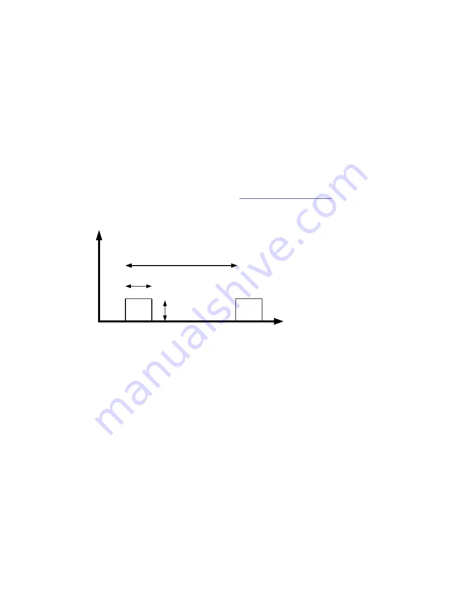
The definition of a minute pulse is that it occurs one minute after the last pulse. As only the flanks

are detected, the flank of the minute pulse shall occur one minute after the last flank.

Binary minute pulses are checked with reference to frequency.

Pulse data:

Period time (a) should be 60 seconds.

Pulse length (b):

Minimum pulse length should be >50 ms.

Maximum pulse length is optional.

Magnitude (c) - please refer to section 

"Binary input module (BIM)"

.

Deviations in the period time (a) larger than 50 ms will cause TSYNCERR.

a

b

c

en05000251.vsd

IEC05000251 V1 EN-US

Figure 631: Binary minute pulses

The default time-out-time for a minute pulse is two minutes, and if no valid minute pulse is

received within two minutes a SYNCERR will be given.

If contact bounce occurs, only the first pulse will be detected as a minute pulse. The next minute

pulse will be registered first 60 s - 50 ms after the last contact bounce.

If the minute pulses are perfect, for example, it is exactly 60 seconds between the pulses, contact

bounces might occur 49 ms after the actual minute pulse without effecting the system. If contact

bounce occurs more than 50 ms, for example, it is less than 59950 ms between the two most

adjacent positive (or negative) flanks, the minute pulse will not be accepted.

Binary synchronization example

M11346-74 v5

An IED is configured to use only binary input for time synchronization, and a valid binary input is

applied to a binary input card. The HMI is used to tell the IED the approximate time, and the

minute pulse is then used to synchronize the IED. Minute pulse means that each pulse occurs one

minute after the previous pulse, so the first pulse is not used at all. The second pulse will probably

be rejected due to the spike filter. The third pulse will give the IED a good time, and will reset the

time so that the fourth pulse will occur on a minute border. After the first three minutes, the time

in the IED will be good if the coarse time is set properly via the HMI or if the RTC backup still keeps

the time since last up-time. If the minute pulse is removed, for example, for an hour, the internal

1MRK 502 066-UUS B

Section 21

Basic IED functions

1251

Technical manual

Summary of Contents for Relion 670 series

Page 1: ... RELION 670 SERIES Generator protection REG670 Version 2 1 ANSI Technical manual ...

Page 2: ......

Page 3: ...Document ID 1MRK 502 066 UUS Issued March 2019 Revision B Product version 2 1 Copyright 2016 ABB All rights reserved ...

Page 4: ...erms of such license This product includes software developed by the OpenSSL Project for use in the OpenSSL Toolkit http www openssl org This product includes cryptographic software written developed by Eric Young eay cryptsoft com and Tim Hudson tjh cryptsoft com Trademarks ABB and Relion are registered trademarks of the ABB Group All other brand or product names mentioned in this document may be...

Page 5: ...product failure would create a risk for harm to property or persons including but not limited to personal injuries or death shall be the sole responsibility of the person or entity applying the equipment and those so responsible are hereby requested to ensure that all measures are taken to exclude or mitigate such risks This document has been carefully checked by ABB but deviations cannot be compl...

Page 6: ...rning electrical equipment for use within specified voltage limits Low voltage directive 2006 95 EC This conformity is the result of tests conducted by ABB in accordance with the product standard EN 60255 26 for the EMC directive and with the product standards EN 60255 1 and EN 60255 27 for the low voltage directive The product is designed in accordance with the international standards of the IEC ...

Page 7: ...ol and monitoring functions 59 2 4 Communication 63 2 5 Basic IED functions 65 Section 3 Analog inputs 67 3 1 Introduction 67 3 2 Function block 67 3 3 Signals 67 3 4 Settings 70 3 5 Monitored data 77 3 6 Operation principle 78 3 7 Technical data 79 Section 4 Binary input and output modules 81 4 1 Binary input 81 4 1 1 Binary input debounce filter 81 4 1 2 Oscillation filter 81 4 1 3 Settings 81 4...

Page 8: ...alternatives 94 5 5 2 1 Functionality 94 5 5 2 2 Status LEDs 94 5 5 2 3 Indication LEDs 95 5 5 3 Function keys 102 5 5 3 1 Functionality 102 5 5 3 2 Operation principle 102 Section 6 Differential protection 105 6 1 Transformer differential protection T2WPDIF and T3WPDIF 87T 105 6 1 1 Identification 105 6 1 2 Functionality 105 6 1 3 Function block 108 6 1 4 Signals 109 6 1 5 Settings 112 6 1 6 Moni...

Page 9: ...ata 165 6 4 Low impedance restricted earth fault protection REFPDIF 87N 166 6 4 1 Identification 166 6 4 2 Functionality 166 6 4 3 Function block 167 6 4 4 Signals 167 6 4 5 Settings 168 6 4 6 Monitored data 169 6 4 7 Operation principle 169 6 4 7 1 Fundamental principles of the restricted ground fault protection 169 6 4 7 2 Restricted ground fault protection low impedance differential protection ...

Page 10: ...02 7 2 6 2 Phase to phase fault 203 7 2 6 3 Three phase faults 205 7 2 6 4 Load encroachment 206 7 2 6 5 Minimum operate currents 209 7 2 6 6 Simplified logic diagrams 209 7 2 7 Technical data 215 7 3 Full scheme distance measuring Mho characteristic ZMHPDIS 21 215 7 3 1 Identification 215 7 3 2 Functionality 215 7 3 3 Function block 216 7 3 4 Signals 216 7 3 5 Settings 217 7 3 6 Operation princip...

Page 11: ...7 6 3 Function block 255 7 6 4 Signals 255 7 6 5 Settings 257 7 6 6 Operation principle 259 7 6 6 1 Full scheme measurement 259 7 6 6 2 Impedance characteristic 260 7 6 6 3 Minimum operating current 264 7 6 6 4 Measuring principles 264 7 6 6 5 Directional impedance element for quadrilateral characteristics 267 7 6 6 6 Simplified logic diagrams 268 7 6 7 Technical data 271 7 7 Phase selection quadr...

Page 12: ...9 High speed distance protection for series compensated lines ZMFCPDIS 21 329 7 9 1 Identification 329 7 9 2 Functionality 329 7 9 3 Function block 330 7 9 4 Signals 331 7 9 5 Settings 333 7 9 6 Monitored data 340 7 9 7 Operation principle 341 7 9 7 1 Filtering 341 7 9 7 2 Distance measuring zones 341 7 9 7 3 Phase selection element 342 7 9 7 4 Directional element 343 7 9 7 5 Fuse failure 344 7 9 ...

Page 13: ...unctionality 388 7 12 3 Function block 388 7 12 4 Signals 388 7 12 5 Settings 389 7 12 6 Monitored data 390 7 12 7 Operation principle 390 7 12 8 Technical data 395 7 13 Sensitive rotor earth fault protection injection based ROTIPHIZ 64R 395 7 13 1 Identification 395 7 13 2 Functionality 395 7 13 3 Function block 396 7 13 4 Signals 396 7 13 5 Settings 397 7 13 6 Monitored data 398 7 13 7 Detailed ...

Page 14: ...ionality 433 7 15 3 Function block 433 7 15 4 Signals 434 7 15 5 Settings 434 7 15 6 Monitored data 436 7 15 7 Operation principle 436 7 15 7 1 Operation principle of zone 1 438 7 15 7 2 Operation principle of zone 2 440 7 15 7 3 Operation principle of zone 3 444 7 15 7 4 Load encroachment 444 7 15 7 5 Under voltage seal in 445 7 15 8 Technical data 446 Section 8 Current protection 447 8 1 Instant...

Page 15: ...uantity within the function 479 8 4 7 2 Internal polarizing 480 8 4 7 3 External polarizing for ground fault function 482 8 4 7 4 Directional detection for ground fault function 482 8 4 7 5 Base quantities within the protection 482 8 4 7 6 Internal ground fault protection structure 483 8 4 7 7 Four residual overcurrent steps 483 8 4 7 8 Directional supervision element with integrated directional c...

Page 16: ... 1 Function inputs 510 8 6 8 Technical data 516 8 7 Thermal overload protection two time constants TRPTTR 49 517 8 7 1 Identification 518 8 7 2 Functionality 518 8 7 3 Function block 518 8 7 4 Signals 518 8 7 5 Settings 519 8 7 6 Monitored data 520 8 7 7 Operation principle 520 8 7 8 Technical data 524 8 8 Breaker failure protection CCRBRF 50BF 524 8 8 1 Identification 524 8 8 2 Functionality 524 ...

Page 17: ... 11 7 1 Low pass filtering 548 8 11 7 2 Calibration of analog inputs 548 8 11 8 Technical data 549 8 12 Directional overpower protection GOPPDOP 32 550 8 12 1 Identification 550 8 12 2 Functionality 550 8 12 3 Function block 551 8 12 4 Signals 551 8 12 5 Settings 552 8 12 6 Monitored data 554 8 12 7 Operation principle 554 8 12 7 1 Low pass filtering 556 8 12 7 2 Calibration of analog inputs 556 8...

Page 18: ...9 8 15 1 7 Technical data 570 8 16 Voltage restrained time overcurrent protection VRPVOC 51V 571 8 16 1 Identification 571 8 16 2 Functionality 571 8 16 3 Function block 572 8 16 4 Signals 572 8 16 5 Settings 573 8 16 6 Monitored data 574 8 16 7 Operation principle 574 8 16 7 1 Measured quantities 574 8 16 7 2 Base quantities 574 8 16 7 3 Overcurrent protection 574 8 16 7 4 Logic diagram 576 8 16 ...

Page 19: ...principle 603 9 1 7 1 Measurement principle 604 9 1 7 2 Time delay 604 9 1 7 3 Blocking 609 9 1 7 4 Design 610 9 1 8 Technical data 611 9 2 Two step overvoltage protection OV2PTOV 59 612 9 2 1 Identification 612 9 2 2 Functionality OV2PTOV 612 9 2 3 Function block 613 9 2 4 Signals 613 9 2 5 Settings 614 9 2 6 Monitored data 616 9 2 7 Operation principle 616 9 2 7 1 Measurement principle 617 9 2 7...

Page 20: ...n measurands 645 9 4 7 5 Overexcitation alarm 646 9 4 7 6 Logic diagram 646 9 4 8 Technical data 647 9 5 Voltage differential protection VDCPTOV 60 647 9 5 1 Identification 647 9 5 2 Functionality 647 9 5 3 Function block 648 9 5 4 Signals 648 9 5 5 Settings 649 9 5 6 Monitored data 649 9 5 7 Operation principle 650 9 5 8 Technical data 651 9 6 100 Stator ground fault protection 3rd harmonic based...

Page 21: ...69 10 1 7 5 Design 669 10 1 8 Technical data 670 10 2 Overfrequency protection SAPTOF 81 671 10 2 1 Identification 671 10 2 2 Functionality 671 10 2 3 Function block 672 10 2 4 Signals 672 10 2 5 Settings 672 10 2 6 Monitored data 673 10 2 7 Operation principle 673 10 2 7 1 Measurement principle 673 10 2 7 2 Time delay 673 10 2 7 3 Blocking 674 10 2 7 4 Design 674 10 2 8 Technical data 675 10 3 Ra...

Page 22: ...nitored data 697 11 1 7 Operation principle 698 11 1 7 1 Measured quantities within CVGAPC 698 11 1 7 2 Base quantities for CVGAPC function 700 11 1 7 3 Built in overcurrent protection steps 700 11 1 7 4 Built in undercurrent protection steps 705 11 1 7 5 Built in overvoltage protection steps 705 11 1 7 6 Built in undervoltage protection steps 705 11 1 7 7 Inadvertent generator energizing 705 11 1...

Page 23: ...732 13 2 6 Monitored data 733 13 2 7 Operation principle 733 13 2 7 1 Zero and negative sequence detection 733 13 2 7 2 Delta current and delta voltage detection 735 13 2 7 3 Dead line detection 738 13 2 7 4 Main logic 739 13 2 8 Technical data 742 13 3 Fuse failure supervision VDSPVC 60 742 13 3 1 Identification 742 13 3 2 Functionality 742 13 3 3 Function block 743 13 3 4 Signals 743 13 3 5 Sett...

Page 24: ... diagram 770 14 2 4 5 Signals 770 14 2 5 Interlocking for bus section breaker A1A2_BS 3 770 14 2 5 1 Identification 771 14 2 5 2 Functionality 771 14 2 5 3 Function block 772 14 2 5 4 Logic diagram 773 14 2 5 5 Signals 774 14 2 6 Interlocking for bus section disconnector A1A2_DC 3 775 14 2 6 1 Identification 776 14 2 6 2 Functionality 776 14 2 6 3 Function block 776 14 2 6 4 Logic diagram 777 14 2...

Page 25: ...0 14 2 11 4 Logic diagram 821 14 2 11 5 Signals 822 14 2 12 Position evaluation POS_EVAL 824 14 2 12 1 Identification 824 14 2 12 2 Functionality 824 14 2 12 3 Function block 824 14 2 12 4 Logic diagram 825 14 2 12 5 Signals 825 14 3 Apparatus control APC 825 14 3 1 Functionality 825 14 3 2 Operation principle 826 14 3 3 Error handling 827 14 3 4 Bay control QCBAY 830 14 3 4 1 Functionality 830 14...

Page 26: ...858 14 3 9 5 Operation principle 858 14 3 9 6 Position supervision 858 14 3 9 7 Command response evaluation 859 14 3 10 Bay reserve QCRSV 860 14 3 10 1 Functionality 860 14 3 10 2 Function block 860 14 3 10 3 Signals 861 14 3 10 4 Settings 862 14 3 10 5 Operation principle 862 14 3 11 Reservation input RESIN 864 14 3 11 1 Functionality 864 14 3 11 2 Function block 864 14 3 11 3 Signals 865 14 3 11...

Page 27: ... 1 Identification 910 14 6 2 Functionality 911 14 6 3 Function block 911 14 6 4 Signals 911 14 6 5 Settings 912 14 6 6 Operation principle 912 14 7 Generic communication function for Double Point indication DPGAPC 913 14 7 1 Identification 913 14 7 2 Functionality 913 14 7 3 Function block 913 14 7 4 Signals 913 14 7 5 Settings 914 14 7 6 Operation principle 914 14 8 Single point generic control 8...

Page 28: ... 940 15 1 7 Technical data 944 15 2 Trip matrix logic TMAGAPC 944 15 2 1 Identification 945 15 2 2 Functionality 945 15 2 3 Function block 945 15 2 4 Signals 946 15 2 5 Settings 947 15 2 6 Operation principle 947 15 2 7 Technical data 948 15 3 Logic for group alarm ALMCALH 949 15 3 1 Identification 949 15 3 2 Functionality 949 15 3 3 Function block 949 15 3 4 Signals 949 15 3 5 Settings 950 15 3 6...

Page 29: ...ter function block INV 958 15 6 3 1 Function block 958 15 6 3 2 Signals 958 15 6 3 3 Technical data 959 15 6 4 Loop delay function block LLD 959 15 6 4 1 Function block 959 15 6 4 2 Signals 959 15 6 4 3 Technical data 959 15 6 5 OR function block OR 960 15 6 5 1 Function block 960 15 6 5 2 Signals 960 15 6 5 3 Technical data 960 15 6 6 Pulse timer function block PULSETIMER 961 15 6 6 1 Function bl...

Page 30: ...69 15 7 2 2 Signals 970 15 7 2 3 Technical data 970 15 7 3 Single point input signal attributes converting function block INDEXTSPQT 970 15 7 3 1 Function block 971 15 7 3 2 Signals 971 15 7 3 3 Technical data 971 15 7 4 Invalid logic function block INVALIDQT 971 15 7 4 1 Function block 972 15 7 4 2 Signals 972 15 7 4 3 Technical data 973 15 7 5 Inverter function block INVERTERQT 973 15 7 5 1 Func...

Page 31: ...ackage 981 15 9 Fixed signals FXDSIGN 982 15 9 1 Identification 982 15 9 2 Functionality 982 15 9 3 Function block 983 15 9 4 Signals 983 15 9 5 Settings 983 15 9 6 Operation principle 983 15 10 Boolean 16 to Integer conversion B16I 984 15 10 1 Identification 984 15 10 2 Function block 984 15 10 3 Signals 984 15 10 4 Monitored data 985 15 10 5 Settings 985 15 10 6 Operation principle 985 15 10 7 T...

Page 32: ... 15 14 3 Function block 996 15 14 4 Signals 996 15 14 5 Settings 996 15 14 6 Operation principle 997 15 15 Elapsed time integrator with limit transgression and overflow supervision TEIGAPC 998 15 15 1 Identification 998 15 15 2 Functionality 999 15 15 3 Function block 999 15 15 4 Signals 999 15 15 5 Settings 1000 15 15 6 Operation principle 1000 15 15 6 1 Operation accuracy 1002 15 15 6 2 Memory s...

Page 33: ...VNMMXU 1039 16 1 7 5 Voltage and current sequence measurements VMSQI CMSQI 1040 16 1 8 Technical data 1040 16 2 Gas medium supervision SSIMG 63 1042 16 2 1 Identification 1042 16 2 2 Functionality 1042 16 2 3 Function block 1042 16 2 4 Signals 1042 16 2 5 Settings 1043 16 2 6 Operation principle 1044 16 2 7 Technical data 1044 16 3 Liquid medium supervision SSIML 71 1045 16 3 1 Identification 1045...

Page 34: ... Settings 1062 16 5 6 Operation principle 1064 16 6 Disturbance report DRPRDRE 1065 16 6 1 Identification 1065 16 6 2 Functionality 1065 16 6 3 Function block 1066 16 6 4 Signals 1067 16 6 5 Settings 1069 16 6 6 Monitored data 1078 16 6 7 Operation principle 1081 16 6 8 Technical data 1088 16 7 Logical signal status report BINSTATREP 1089 16 7 1 Identification 1089 16 7 2 Functionality 1089 16 7 3...

Page 35: ...nical data 1100 Section 17 Metering 1101 17 1 Pulse counter logic PCFCNT 1101 17 1 1 Identification 1101 17 1 2 Functionality 1101 17 1 3 Function block 1101 17 1 4 Signals 1102 17 1 5 Settings 1102 17 1 6 Monitored data 1103 17 1 7 Operation principle 1103 17 1 8 Technical data 1105 17 2 Function for energy calculation and demand handling ETPMMTR 1105 17 2 1 Identification 1105 17 2 2 Functionali...

Page 36: ...119 18 4 6 3 Signals 1119 18 4 6 4 Settings 1119 18 4 6 5 Monitored data 1120 18 4 6 6 Operation principle 1120 18 4 7 IEC 61850 8 1 redundant station bus communication 1120 18 4 7 1 Functionality 1121 18 4 7 2 Function block 1121 18 4 7 3 Signals 1121 18 4 7 4 Settings 1121 18 4 7 5 Monitored data 1122 18 4 7 6 Principle of operation 1122 18 5 IEC 61850 9 2LE communication protocol 1123 18 5 1 In...

Page 37: ...tings 1164 18 8 4 Function status auto recloser for IEC 60870 5 103 I103AR 1165 18 8 4 1 Functionality 1165 18 8 4 2 Identification 1165 18 8 4 3 Function block 1165 18 8 4 4 Signals 1166 18 8 4 5 Settings 1166 18 8 5 Function status ground fault for IEC 60870 5 103 I103EF 1166 18 8 5 1 Functionality 1166 18 8 5 2 Identification 1166 18 8 5 3 Function block 1166 18 8 5 4 Signals 1167 18 8 5 5 Sett...

Page 38: ... IEC 60870 5 103 I103IEDCMD 1175 18 8 11 1 Functionality 1175 18 8 11 2 Identification 1175 18 8 11 3 Function block 1176 18 8 11 4 Signals 1176 18 8 11 5 Settings 1176 18 8 12 Function commands user defined for IEC 60870 5 103 I103USRCMD 1176 18 8 12 1 Functionality 1176 18 8 12 2 Identification 1177 18 8 12 3 Function block 1177 18 8 12 4 Signals 1177 18 8 12 5 Settings 1178 18 8 13 Function com...

Page 39: ...7 18 10 4 Operation principle 1198 18 11 GOOSE function block to receive a double point value GOOSEDPRCV 1198 18 11 1 Identification 1198 18 11 2 Functionality 1199 18 11 3 Function block 1199 18 11 4 Signals 1199 18 11 5 Settings 1199 18 11 6 Operation principle 1199 18 12 GOOSE function block to receive an integer value GOOSEINTRCV 1200 18 12 1 Identification 1200 18 12 2 Functionality 1200 18 1...

Page 40: ...17 6 Operation principle 1208 18 18 Security events on protocols SECALARM 1209 18 18 1 Security alarm SECALARM 1209 18 18 1 1 Signals 1209 18 18 1 2 Settings 1209 18 19 Activity logging parameters ACTIVLOG 1209 18 19 1 Activity logging ACTIVLOG 1209 18 19 2 Settings 1209 Section 19 Remote communication 1211 19 1 Binary signal transfer 1211 19 1 1 Identification 1211 19 1 2 Functionality 1211 19 1 ...

Page 41: ...0 4 6 Operation principle 1227 20 5 Self supervision with internal event list INTERRSIG 1227 20 5 1 Functionality 1227 20 5 2 Function block 1227 20 5 3 Signals 1228 20 5 4 Settings 1228 20 5 5 Operation principle 1228 20 5 5 1 Internal signals 1229 20 5 5 2 Supervision of analog inputs 1231 20 5 6 Technical data 1231 20 6 ChangeLock function CHNGLCK 1232 20 6 1 Functionality 1232 20 6 2 Function ...

Page 42: ...tings 1256 21 3 5 Operation principle 1257 21 4 IED identifiers 1257 21 4 1 Functionality 1257 21 4 2 Settings 1258 21 5 Product information 1258 21 5 1 Functionality 1258 21 5 2 Settings 1258 21 5 3 Factory defined settings 1259 21 6 Signal matrix for binary inputs SMBI 1259 21 6 1 Functionality 1259 21 6 2 Function block 1260 21 6 3 Signals 1260 21 6 4 Operation principle 1261 21 7 Signal matrix...

Page 43: ...272 Section 22 IED hardware 1273 22 1 Overview 1273 22 1 1 Variants of case size with local HMI display 1273 22 1 2 Case from the rear side 1275 22 2 Hardware modules 1280 22 2 1 Overview 1280 22 2 2 Numeric processing module NUM 1280 22 2 2 1 Introduction 1280 22 2 2 2 Functionality 1281 22 2 2 3 Block diagram 1282 22 2 3 Power supply module PSM 1282 22 2 3 1 Introduction 1282 22 2 3 2 Design 128...

Page 44: ...d data 1303 22 2 9 6 Technical data 1305 22 2 10 Binary input output module IOM 1307 22 2 10 1 Introduction 1307 22 2 10 2 Design 1307 22 2 10 3 Signals 1309 22 2 10 4 Settings 1310 22 2 10 5 Monitored data 1310 22 2 10 6 Technical data 1312 22 2 11 mA input module MIM 1315 22 2 11 1 Introduction 1315 22 2 11 2 Design 1315 22 2 11 3 Signals 1316 22 2 11 4 Settings 1317 22 2 11 5 Monitored data 131...

Page 45: ...ction 1330 22 2 18 2 Design 1330 22 2 18 3 Technical data 1332 22 2 19 IRIG B time synchronization module IRIG B 1332 22 2 19 1 Introduction 1332 22 2 19 2 Design 1332 22 2 19 3 Settings 1333 22 2 19 4 Technical data 1333 22 3 Dimensions 1334 22 3 1 Case without rear cover 1334 22 3 2 Case with rear cover 1336 22 3 3 Flush mounting dimensions 1338 22 3 4 Side by side flush mounting dimensions 1339...

Page 46: ...ion 23 Injection equipment hardware 1357 23 1 Overview 1357 23 1 1 Front view of injection unit coupling capacitor and shunt resitor unit 1357 23 1 1 1 Injection unit REX060 1357 23 1 1 2 REX060 Front panel controls 1358 23 1 1 3 Coupling capacitor unit REX061 1359 23 1 1 4 Shunt resistor unit REX062 1361 23 1 2 Injection unit REX060 from rear side 1362 23 1 2 1 Injection unit REX060 1362 23 2 Inj...

Page 47: ... Connection diagrams 1379 Section 26 Inverse time characteristics 1381 26 1 Application 1381 26 2 Principle of operation 1383 26 2 1 Mode of operation 1383 26 3 Inverse characteristics 1388 Section 27 Glossary 1417 Table of contents 41 Technical manual ...

Page 48: ...42 ...

Page 49: ...ng normal service 1 2 Intended audience GUID C9B8127F 5748 4BEA 9E4F CC762FE28A3A v10 This manual addresses system engineers and installation and commissioning personnel who use technical data during engineering installation and commissioning and in normal service The system engineer must have a thorough knowledge of protection systems protection equipment protection functions and the configured f...

Page 50: ... LHMI functions as well as communication engineering for IEC 60870 5 103 IEC 61850 DNP3 LON and SPA The installation manual contains instructions on how to install the IED The manual provides procedures for mechanical and electrical installation The chapters are organized in the chronological order in which the IED should be installed The commissioning manual contains instructions on how to commis...

Page 51: ...tlook and properties of the data points specific to the IED The manual should be used in conjunction with the corresponding communication protocol manual The cyber security deployment guideline describes the process for handling cyber security when communicating with the IED Certification Authorization with role based access control and product engineering for cyber security related events are des...

Page 52: ...or warning about the temperature of product surfaces Class 1 Laser product Take adequate measures to protect the eyes and do not view directly with optical instruments The caution icon indicates important information or warning related to the concept discussed in the text It might indicate the presence of a hazard which could result in corruption of software or damage to equipment or property The ...

Page 53: ...lines In a logic diagram input and output signal paths are shown as lines that touch the outer border of the diagram Input signals are always on the left hand side and output signals are on the right hand side Input and output signals can be configured using PCM600 They can be connected to the inputs and outputs of other functions and to binary inputs and outputs Examples of input signals are BLKT...

Page 54: ...BCZTPDIF BDCGAPC SWSGGIO BBCSWI BDCGAPC BRCPTOC BRCPTOC BRCPTOC BRPTOC BRPTOC BRPTOC BTIGAPC B16IFCVI BTIGAPC BUSPTRC_B1 BUSPTRC BBSPLLN0 BUSPTRC BUSPTRC_B2 BUSPTRC BUSPTRC BUSPTRC_B3 BUSPTRC BUSPTRC BUSPTRC_B4 BUSPTRC BUSPTRC BUSPTRC_B5 BUSPTRC BUSPTRC BUSPTRC_B6 BUSPTRC BUSPTRC BUSPTRC_B7 BUSPTRC BUSPTRC BUSPTRC_B8 BUSPTRC BUSPTRC BUSPTRC_B9 BUSPTRC BUSPTRC BUSPTRC_B10 BUSPTRC BUSPTRC BUSPTRC_B1...

Page 55: ...UTPTRC BUTPTRC BZISGGIO BZISGGIO BZISGAPC BZITGGIO BZITGGIO BZITGAPC BZNSPDIF_A BZNSPDIF BZASGAPC BZASPDIF BZNSGAPC BZNSPDIF BZNSPDIF_B BZNSPDIF BZBSGAPC BZBSPDIF BZNSGAPC BZNSPDIF BZNTPDIF_A BZNTPDIF BZATGAPC BZATPDIF BZNTGAPC BZNTPDIF BZNTPDIF_B BZNTPDIF BZBTGAPC BZBTPDIF BZNTGAPC BZNTPDIF CBPGAPC CBPLLN0 CBPMMXU CBPPTRC HOLPTOV HPH1PTOV PH3PTUC PH3PTOC RP3PDOP CBPMMXU CBPPTRC HOLPTOV HPH1PTOV P...

Page 56: ...CRWPSCH EF2PTOC EF2LLN0 EF2PTRC EF2RDIR GEN2PHAR PH1PTOC EF2PTRC EF2RDIR GEN2PHAR PH1PTOC EF4PTOC EF4LLN0 EF4PTRC EF4RDIR GEN4PHAR PH1PTOC EF4PTRC EF4RDIR GEN4PHAR PH1PTOC EFPIOC EFPIOC EFPIOC EFRWPIOC EFRWPIOC EFRWPIOC ETPMMTR ETPMMTR ETPMMTR FDPSPDIS FDPSPDIS FDPSPDIS FMPSPDIS FMPSPDIS FMPSPDIS FRPSPDIS FPSRPDIS FPSRPDIS FTAQFVR FTAQFVR FTAQFVR FUFSPVC SDDRFUF FUFSPVC SDDSPVC GENPDIF GENPDIF GEN...

Page 57: ... L6CGAPC L6CPDIF L6CPHAR L6CPTRC LAPPGAPC LAPPLLN0 LAPPPDUP LAPPPUPF LAPPPDUP LAPPPUPF LCCRPTRC LCCRPTRC LCCRPTRC LCNSPTOC LCNSPTOC LCNSPTOC LCNSPTOV LCNSPTOV LCNSPTOV LCP3PTOC LCP3PTOC LCP3PTOC LCP3PTUC LCP3PTUC LCP3PTUC LCPTTR LCPTTR LCPTTR LCZSPTOC LCZSPTOC LCZSPTOC LCZSPTOV LCZSPTOV LCZSPTOV LD0LLN0 LLN0 LDLPSCH LDLPDIF LDLPSCH LDRGFC STSGGIO LDRGFC LEXPDIS LEXPDIS LEXPDIS LEXPTRC LFPTTR LFPTT...

Page 58: ...PTOC PH3PTRC GEN4PHAR PH3PTOC PH3PTRC OEXPVPH OEXPVPH OEXPVPH OOSPPAM OOSPPAM OOSPPAM OOSPTRC OV2PTOV GEN2LLN0 OV2PTOV PH1PTRC OV2PTOV PH1PTRC PAPGAPC PAPGAPC PAPGAPC PCFCNT PCGGIO PCFCNT PH4SPTOC GEN4PHAR OCNDLLN0 PH1BPTOC PH1PTRC GEN4PHAR PH1BPTOC PH1PTRC PHPIOC PHPIOC PHPIOC PRPSTATUS RCHLCCH RCHLCCH SCHLCCH PSLPSCH ZMRPSL PSLPSCH PSPPPAM PSPPPAM PSPPPAM PSPPTRC QCBAY QCBAY QCRSV QCRSV QCRSV RE...

Page 59: ...PTRC SMPPTRC SP16GAPC SP16GGIO SP16GAPC SPC8GAPC SPC8GGIO SPC8GAPC SPGAPC SPGGIO SPGAPC SSCBR SSCBR SSCBR SSIMG SSIMG SSIMG SSIML SSIML SSIML STBPTOC STBPTOC BBPMSS STBPTOC STEFPHIZ STEFPHIZ STEFPHIZ STTIPHIZ STTIPHIZ STTIPHIZ SXCBR SXCBR SXCBR SXSWI SXSWI SXSWI T2WPDIF T2WPDIF T2WGAPC T2WPDIF T2WPHAR T2WPTRC T3WPDIF T3WPDIF T3WGAPC T3WPDIF T3WPHAR T3WPTRC TCLYLTC TCLYLTC TCLYLTC TCSLTC TCMYLTC TC...

Page 60: ...GIO VSGAPC WRNCALH WRNCALH WRNCALH ZC1PPSCH ZPCPSCH ZPCPSCH ZC1WPSCH ZPCWPSCH ZPCWPSCH ZCLCPSCH ZCLCPLAL ZCLCPSCH ZCPSCH ZCPSCH ZCPSCH ZCRWPSCH ZCRWPSCH ZCRWPSCH ZCVPSOF ZCVPSOF ZCVPSOF ZGVPDIS ZGVLLN0 PH1PTRC ZGVPDIS ZGVPTUV PH1PTRC ZGVPDIS ZGVPTUV ZMCAPDIS ZMCAPDIS ZMCAPDIS ZMCPDIS ZMCPDIS ZMCPDIS ZMFCPDIS ZMFCLLN0 PSFPDIS ZMFPDIS ZMFPTRC ZMMMXU PSFPDIS ZMFPDIS ZMFPTRC ZMMMXU ZMFPDIS ZMFLLN0 PSF...

Page 61: ... nodes Edition 2 logical nodes ZMQAPDIS ZMQAPDIS ZMQAPDIS ZMQPDIS ZMQPDIS ZMQPDIS ZMRAPDIS ZMRAPDIS ZMRAPDIS ZMRPDIS ZMRPDIS ZMRPDIS ZMRPSB ZMRPSB ZMRPSB ZSMGAPC ZSMGAPC ZSMGAPC 1MRK 502 066 UUS B Section 1 Introduction 55 Technical manual ...

Page 62: ...56 ...

Page 63: ...one quadrilateral characteristic ZDRDIR 21D Directional impedance quadrilateral FDPSPDIS 21 Phase selection quadrilateral characteristic with fixed angle ZMHPDIS 21 Fullscheme distance protection mho characteristic 0 4 ZDMRDIR 21D Directional impedance element for mho characteristic 0 2 FMPSPDIS 21 Faulty phase identification with load enchroachment ZMRPDIS ZMRAPDIS 21 Distance protection zone qua...

Page 64: ...uence overcurrent protection 0 2 SDEPSDE 67N Sensitive directional residual overcurrent and power protection 0 2 TRPTTR 49 Thermal overload protection two time constant 0 3 CCRBRF 50BF Breaker failure protection 0 4 STBPTOC 50STB Stub protection CCPDSC 52PD Pole discordance protection 0 4 GUPPDUP 37 Directional underpower protection 0 4 GOPPDOP 32 Directional overpower protection 0 4 BRCPTOC 46 Br...

Page 65: ...ing functions GUID E3777F16 0B76 4157 A3BF 0B6B978863DE v12 IEC 61850 ANSI Function description Generator REG670 Control SESRSYN 25 Synchrocheck energizing check and synchronizing 0 2 APC15 3 Apparatus control for single bay max 15 apparatuses 2CBs incl interlocking APC30 3 Apparatus control for up to 6 bays max 30 apparatuses 6CBs incl interlocking 0 1 QCBAY Apparatus control 1 5 APC30 LOCREM Han...

Page 66: ...0 5 103 50 I103POSCMDV IED direct commands with position for IEC 60870 5 103 10 I103IEDCMD IED commands for IEC 60870 5 103 1 I103USRCMD Function commands user defined for IEC 60870 5 103 1 Secondary system supervision CCSSPVC 87 Current circuit supervision 0 5 FUFSPVC Fuse failure supervision 0 3 VDSPVC 60 Fuse failure supervision based on voltage difference 0 3 Logic SMPPTRC 94 Tripping logic 12...

Page 67: ...gnal integration 30 TEIGAPC Elapsed time integrator with limit transgression and overflow supervision 12 INTCOMP Comparator for integer inputs 12 REALCOMP Comparator for real inputs 12 Monitoring CVMMXN VMMXU CMSQI VMSQI VNMMXU Measurements 6 CMMXU Measurements 10 AISVBAS Function block for service value presentation of secondary analog inputs 1 EVENT Event function 20 DRPRDRE A1RADR A4RADR B1RBDR...

Page 68: ...60870 5 103 1 I103IED IED status for IEC 60870 5 103 1 I103SUPERV Supervison status for IEC 60870 5 103 1 I103USRDEF Status for user defined signals for IEC 60870 5 103 20 L4UFCNT Event counter with limit supervision 30 TEILGAPC Running hour meter 9 Metering PCFCNT Pulse counter logic 16 ETPMMTR Function for energy calculation and demand handling 6 Table 3 Total number of instances for basic confi...

Page 69: ...tances AND 180 GATE 49 INV 180 LLD 49 OR 180 PULSETIMER 59 SLGAPC 74 SRMEMORY 110 TIMERSET 49 VSGAPC 130 XOR 49 2 4 Communication GUID 5F144B53 B9A7 4173 80CF CD4C84579CB5 v12 IEC 61850 ANSI Function description Generator REG670 Customized Station communication LONSPA SPA SPA communication protocol 1 ADE LON communication protocol 1 HORZCOMM Network variables via LON 1 PROTOCOL Operation selection...

Page 70: ...OSEMVRCV GOOSE function block to receive a measurand value 60 GOOSESPRCV GOOSE function block to receive a single point value 64 MULTICMDRCV MULTICMDSND Multiple command and transmit 60 10 FRONT LANABI LANAB LANCDI LANCD Ethernet configuration of links 1 GATEWAY Ethernet configuration of link one 1 OPTICAL103 IEC 60870 5 103 Optical serial communication 1 RS485103 IEC 60870 5 103 serial communicat...

Page 71: ... synchronization module BININPUT SYNCHCAN SYNCHGPS SYNCHCMPPS SYNCHLON SYNCHPPH SYNCHPPS SNTP SYNCHSPA Time synchronization TIMEZONE Time synchronization DSTBEGIN DSTENABLE DSTEND GPS time synchronization module IRIG B Time synchronization SETGRPS Number of setting groups ACTVGRP Parameter setting groups TESTMODE Test mode functionality CHNGLCK Change lock function SMBI Signal matrix for binary in...

Page 72: ...ation RUNTIME IED Runtime Comp CAMCONFIG Central account management configuration CAMSTATUS Central account management status TOOLINF Tools Information component SAFEFILECOPY Safe file copy function Table 7 Local HMI functions IEC 61850 or function name ANSI Description LHMICTRL Local HMI signals LANGUAGE Local human machine language SCREEN Local HMI Local human machine screen behavior FNKEYTY1 FN...

Page 73: ...grees and all other angle information will be shown in relation to this analog input During testing and commissioning of the IED the reference channel can be changed to facilitate testing and service values reading The availability of VT inputs depends on the ordered transformer input module TRM type 3 2 Function block SEMOD116577 1 v4 The hardware channels appear in the signal matrix tool SMT and...

Page 74: ...ING Analog current input 4 CH5 I STRING Analog current input 5 CH6 I STRING Analog current input 6 CH7 V STRING Analog voltage input 7 CH8 V STRING Analog voltage input 8 CH9 V STRING Analog voltage input 9 CH10 V STRING Analog voltage input 10 CH 11 V STRING Analog voltage input 11 CH12 V STRING Analog voltage input 12 PID 3922 OUTPUTSIGNALS v4 Table 10 TRM_6I Output signals Name Type Description...

Page 75: ... Output signals Name Type Description STATUS BOOLEAN Analog input module status CH1 I STRING Analogue current input 1 CH2 I STRING Analog current input 2 CH3 I STRING Analog current input 3 CH4 I STRING Analog current input 4 CH5 I STRING Analog current input 5 CH6 I STRING Analog current input 6 CH7 I STRING Analog current input 7 CH8 I STRING Analog current input 8 CH9 I STRING Analog current in...

Page 76: ...t 12 3 4 Settings SEMOD129840 4 v2 Dependent on ordered IED type PID 4153 SETTINGS v8 Table 14 AISVBAS Non group settings basic Name Values Range Unit Step Default Description PhaseAngleRef TRM40 Ch1 Ch12 TRM41 Ch1 Ch12 MU1 IA I0 MU1 VA V0 MU2 IA I0 MU2 VA V0 MU3 IA I0 MU3 VA V0 MU4 IA I0 MU4 VA V0 MU5 IA I0 MU5 VA V0 MU6 IA I0 MU6 VA V0 MU7 IA I0 MU7 VA V0 MU8 IA I0 MU8 VA V0 MU9 IA I0 MU9 VA V0 ...

Page 77: ... the opposite CTsec5 1 10 A 1 1 Rated CT secondary current CTprim5 1 99999 A 1 3000 Rated CT primary current CT_WyePoint6 FromObject ToObject ToObject ToObject towards protected object FromObject the opposite CTsec6 1 10 A 1 1 Rated CT secondary current CTprim6 1 99999 A 1 3000 Rated CT primary current CT_WyePoint7 FromObject ToObject ToObject ToObject towards protected object FromObject the oppos...

Page 78: ...t towards protected object FromObject the opposite CTsec3 1 10 A 1 1 Rated CT secondary current CTprim3 1 99999 A 1 3000 Rated CT primary current CT_WyePoint4 FromObject ToObject ToObject ToObject towards protected object FromObject the opposite CTsec4 1 10 A 1 1 Rated CT secondary current CTprim4 1 99999 A 1 3000 Rated CT primary current CT_WyePoint5 FromObject ToObject ToObject ToObject towards ...

Page 79: ...towards protected object FromObject the opposite CTsec2 1 10 A 1 1 Rated CT secondary current CTprim2 1 99999 A 1 3000 Rated CT primary current CT_WyePoint3 FromObject ToObject ToObject ToObject towards protected object FromObject the opposite CTsec3 1 10 A 1 1 Rated CT secondary current CTprim3 1 99999 A 1 3000 Rated CT primary current CT_WyePoint4 FromObject ToObject ToObject ToObject towards pr...

Page 80: ...pposite CTsec5 1 10 A 1 1 Rated CT secondary current CTprim5 1 99999 A 1 3000 Rated CT primary current CT_WyePoint6 FromObject ToObject ToObject ToObject towards protected object FromObject the opposite CTsec6 1 10 A 1 1 Rated CT secondary current CTprim6 1 99999 A 1 3000 Rated CT primary current CT_WyePoint7 FromObject ToObject ToObject ToObject towards protected object FromObject the opposite CT...

Page 81: ...ject the opposite CTsec5 1 10 A 1 1 Rated CT secondary current CTprim5 1 99999 A 1 3000 Rated CT primary current CT_WyePoint6 FromObject ToObject ToObject ToObject towards protected object FromObject the opposite CTsec6 1 10 A 1 1 Rated CT secondary current CTprim6 1 99999 A 1 3000 Rated CT primary current CT_WyePoint7 FromObject ToObject ToObject ToObject towards protected object FromObject the o...

Page 82: ...ject ToObject towards protected object FromObject the opposite CTsec4 1 10 A 1 1 Rated CT secondary current CTprim4 1 99999 A 1 3000 Rated CT primary current CT_WyePoint5 FromObject ToObject ToObject ToObject towards protected object FromObject the opposite CTsec5 1 10 A 1 1 Rated CT secondary current CTprim5 1 99999 A 1 3000 Rated CT primary current CT_WyePoint6 FromObject ToObject ToObject ToObj...

Page 83: ...T primary voltage 3 5 Monitored data PID 4153 MONITOREDDATA v4 Table 21 AISVBAS Monitored data Name Type Values Range Unit Description Status INTEGER 0 Ok 1 Error 2 AngRefLow 3 Uncorrelated Service value status PID 3920 MONITOREDDATA v4 Table 22 TRM_12I Monitored data Name Type Values Range Unit Description STATUS BOOLEAN 0 Ok 1 Error Analog input module status PID 3921 MONITOREDDATA v4 Table 23 T...

Page 84: ...of a current depends on the connection of the CT The main CTs are typically star WYE connected and can be connected with the Star WYE point towards the object or away from the object This information must be set in the IED The convention of the directionality is defined as follows Positive value of current or power means that the quantity has the direction into the object Negative value of current...

Page 85: ...tings of the IED is performed in primary values The ratios of the main CTs and VTs are therefore basic data for the IED The user has to set the rated secondary and primary currents and voltages of the CTs and VTs to provide the IED with their rated ratios The CT and VT ratio and the name on respective channel is done under Main menu Hardware Analog modules in the Parameter Settings tool or on the ...

Page 86: ... s 10 Ir for 1 min 1 8 Ir for 30 min 1 1 Ir continuously 65 Ir for 1 s 20 Ir for 10 s 8 Ir for 1 min 1 6 Ir for 30 min 1 1 Ir continuously Burden 200 mVA at Ir 350 mVA at Ir Voltage inputs Rated voltage Ur 110 or 220 V Operating range 0 340 V Thermal withstand 450 V for 10 s 420 V continuously Burden 20 mVA at 110 V 80 mVA at 220 V all values for individual voltage inputs Note All current and volt...

Page 87: ...lectromagnetic fields from for example nearby breakers An oscillation filter is used to reduce the disturbance from the system when a binary input starts oscillating An oscillation counter counts the debounced signal state changes during 1 s If the counter value is greater than the set value OscBlock the input signal is blocked The input signal is ignored until the oscillation counter value during...

Page 88: ...ult Description Operation Disabled Enabled Enabled Binary input output module in operation On or not Off DebounceTime 0 001 0 020 s 0 001 0 001 Debounce time for binary inputs OscBlock 1 40 Hz 1 40 Oscillation block limit OscRelease 1 30 Hz 1 30 Oscillation release limit Section 4 1MRK 502 066 UUS B Binary input and output modules 82 Technical manual ...

Page 89: ... for display DefaultScreen 0 Default screen EvListSrtOrder Latest on top Oldest on top Latest on top Sort order of event list AutoIndicationDRP Disabled Enabled Disabled Automatic indication of disturbance report SubstIndSLD No Yes No Substitute indication on single line diagram InterlockIndSLD No Yes No Interlock indication on single line diagram BypassCommands No Yes No Enable bypass of commands...

Page 90: ...n the LCD HMI is steady YELLOW S BOOLEAN Yellow LED on the LCD HMI is steady YELLOW F BOOLEAN Yellow LED on the LCD HMI is flashing RSTPULSE BOOLEAN A reset pulse is provided when the LEDs on the LCD HMI are cleared LEDSRST BOOLEAN Active when the LEDs on the LCD HMI are not ON 5 3 Basic part for LED indication module 5 3 1 Identification GUID 6E36C0BC F284 4C88 A4A8 9535D3BE8B14 v2 Function descr...

Page 91: ...nput to block the operation of the LEDs RESET BOOLEAN 0 Input to acknowledge reset the indication LEDs PID 4114 OUTPUTSIGNALS v4 Table 37 LEDGEN Output signals Name Type Description NEWIND BOOLEAN New indication signal if any LED indication input is set ACK BOOLEAN A pulse is provided when the LEDs are acknowledged PID 1697 INPUTSIGNALS v16 Table 38 GRP1_LED1 Input signals Name Type Default Descri...

Page 92: ...wn when LED 1 alarm group 1 is off LabelRed 0 18 1 G1L01_RED Label string shown when LED 1 alarm group 1 is red LabelYellow 0 18 1 G1L01_YELLOW Label string shown when LED 1 alarm group 1 is yellow LabelGreen 0 18 1 G1L01_GREEN Label string shown when LED 1 alarm group 1 is green 5 4 LCD part for HMI function keys control module GUID EECAE7FA 7078 472C A429 F7607DB884EB v2 5 4 1 Identification GUI...

Page 93: ... Default Description Mode Disabled Toggle Pulsed Disabled Output operation mode PulseTime 0 001 60 000 s 0 001 0 200 Pulse time for output controlled by LCDFn1 LabelOn 0 18 1 LCD_FN1_ON Label for LED on state LabelOff 0 18 1 LCD_FN1_OFF Label for LED off state PID 6327 SETTINGS v1 Table 44 FNKEYTY1 Non group settings basic Name Values Range Unit Step Default Description Type Disabled Menu shortcut...

Page 94: ...US Figure 10 Local human machine interface The LHMI of the IED contains the following elements Keypad Display LCD LED indicators Communication port for PCM600 The LHMI is used for setting monitoring and controlling Section 5 1MRK 502 066 UUS B Local Human Machine Interface LHMI 88 Technical manual ...

Page 95: ...push buttons are also used to acknowledge alarms reset indications provide help and switch between local and remote control mode The keypad also contains programmable push buttons that can be configured either as menu shortcut or control buttons 1MRK 502 066 UUS B Section 5 Local Human Machine Interface LHMI 89 Technical manual ...

Page 96: ... object control navigation and command push buttons and RJ 45 communication port 1 5 Function button 6 Close 7 Open 8 Escape 9 Left 10 Down 11 Up 12 Right 13 Key 14 Enter 15 Remote Local 16 Uplink LED 17 Not in use 18 Multipage 19 Menu 20 Clear 21 Help Section 5 1MRK 502 066 UUS B Local Human Machine Interface LHMI 90 Technical manual ...

Page 97: ... monochrome liquid crystal display LCD with a resolution of 320 x 240 pixels The character size can vary The display view is divided into four basic areas IEC15000270 1 en vsdx IEC15000270 V1 EN US Figure 12 Display layout 1 Path 2 Content 3 Status 4 Scroll bar appears when needed 1MRK 502 066 UUS B Section 5 Local Human Machine Interface LHMI 91 Technical manual ...

Page 98: ... content area is truncated from the beginning if it does not fit in the display horizontally Truncation is indicated with three dots IEC15000138 1 en vsdx IEC15000138 V1 EN US Figure 13 Truncated path The number after colon sign at the end of the function instance for example 1 in SMAI1 1 indicates the number of that function instance The function key button panel shows on request what actions are...

Page 99: ... Indication LED panel The function button and indication LED panels are not visible at the same time Each panel is shown by pressing one of the function buttons or the Multipage button Pressing the ESC button clears the panel from the display Both panels have a dynamic width that depends on the label string length 5 5 1 3 LEDs AMU0600427 v12 The LHMI includes three protection status LEDs above the...

Page 100: ...l LEDs which are next to the control buttons and They can for example represent the status of a circuit breaker The LEDs are controlled by the function block OPENCLOSE_LED which must be configured to show the status of the breaker 5 5 2 LED configuration alternatives 5 5 2 1 Functionality GUID 1A03E0EF C10F 4797 9D9F 5CCA86CA29EB v5 The function blocks LEDGEN and GRP1_LEDx GRP2_LEDx and GRP3_LEDx ...

Page 101: ... is not possible to get a clear view of what triggered the latest event without looking at the sequence of events list A condition for getting the sequence of events is that the signals have been engineered in the disturbance recorder Re starting mode In the re starting mode of operation each new pickup resets all previous active LEDs and activates only those which appear during one disturbance On...

Page 102: ...LatchedReset S For sequence 1 and 2 which are of the Follow type the acknowledgment Ack reset function is not applicable because the indication shown by the LED follows its input signal Sequence 3 and 4 which are of the Latched type with acknowledgement are only working in collecting Coll mode Sequence 5 is working according to Latched type and collecting mode while Sequence 6 is working according...

Page 103: ...low F SEMOD56072 47 v2 This sequence is the same as Sequence 1 Follow S but the LEDs are flashing instead of showing steady light Sequence 3 LatchedAck F S SEMOD56072 50 v2 This sequence has a latched function and works in collecting mode Every LED is independent of the other LEDs in its operation At the activation of the input signal the indication starts flashing After acknowledgment the indicat...

Page 104: ... IEC09000313 V1 EN US Figure 20 Operating Sequence 3 LatchedAck F S 2 colors involved GUID A652A49D F016 472D 8D38 6D3E75DAB1DB v2 If all three signals are activated the order of priority is still maintained Acknowledgment of indications with higher priority will acknowledge also low priority indications which are not visible according to Figure 21 Activating signal RED LED Acknow IEC09000314 1 en...

Page 105: ...light The difference to sequence 3 and 4 is that indications that are still activated will not be affected by the reset that is immediately after the positive edge of the reset has been executed a new reading and storing of active signals is performed Every LED is independent of the other LEDs in its operation IEC01000235_2_en vsd Activating signal LED Reset IEC01000235 V2 EN US Figure 23 Operatin...

Page 106: ...f that the manual reset has been executed a new reading and storing of active signals is performed LEDs set for sequence 6 are completely independent in its operation of LEDs set for other sequences Timing diagram for sequence 6 SEMOD56072 86 v3 Figure 25 shows the timing diagram for two indications within one disturbance IEC01000239_2 en vsd Activating signal 2 LED 2 Manual reset Activating signa...

Page 107: ...ication appears after the first one has reset but before tRestart has elapsed IEC01000241_2_en vsd Activating signal 2 LED 2 Manual reset Activating signal 1 Automatic reset LED 1 Disturbance tRestart IEC01000241 V2 EN US Figure 27 Operating sequence 6 LatchedReset S two indications within same disturbance but with reset of activating signal between Figure 28 shows the timing diagram for manual re...

Page 108: ...l a binary signal 5 5 3 2 Operation principle GUID 977C3829 B19B 457E 8A4D 45317226EF22 v3 Each output on the FNKEYMD1 FNKEYMD5 function blocks can be controlled from the LHMI function keys By pressing a function button on the LHMI the output status of the actual function block will change These binary outputs can in turn be used to control other function blocks for example switch control blocks b...

Page 109: ...ut sets high 1 when the function key has been pressed for more than 500ms and remains high according to set pulse time After this time the output will go back to 0 The input attribute is reset when the function block detects it being high and there is no output pulse Note that the third positive edge on the input attribute does not cause a pulse since the edge was applied during pulse output A new...

Page 110: ...ock becomes active and will light the yellow function button LED when high This functionality is active even if the function block operation setting is set to off It has been implemented this way for safety reasons the idea is that the function key LEDs should always reflect the actual status of any primary equipment monitored by these LEDs Section 5 1MRK 502 066 UUS B Local Human Machine Interfac...

Page 111: ...ferential protection is provided with internal CT ratio matching phase shift compensation and settable zero sequence current elimination The function can be provided with up to six three phase sets of current inputs if enough HW is available All current inputs are provided with percentage bias restraint features making the IED suitable for two or three winding transformer in multi breaker station ...

Page 112: ...xx05000051_ansi vsd 252 152 352 452 ANSI05000051 V1 EN US two winding power transformer with two circuit breakers and two CT sets on both sides Three winding applications xx05000052_ansi vsd 352 152 452 ANSI05000052 V1 EN US three winding power transformer with all three windings connected Table continues on next page Section 6 1MRK 502 066 UUS B Differential protection 106 Technical manual ...

Page 113: ...h fault currents By introducing the load tap changer position the differential protection pick up can be set to optimum sensitivity thus covering internal faults with low fault current level Harmonic restraint is included for inrush and overexcitation currents respectively cross blocking is also available Adaptive stabilization is also included for system recovery inrush and CT saturation during e...

Page 114: ...KNSSEN TRIP TRIPRES TRIPUNRE TRNSUNR TRNSSENS PICKUP PU_A PU_B PU_C BLK2H BLK2H_A BLK2H_B BLK2H_C BLK5H BLK5H_A BLK5H_B BLK5H_C BLKWAV BLKWAV_A BLKWAV_B BLKWAV_C IDALARM OPENCT OPENCTAL ID_A ID_B ID_C IDMAG_A IDMAG_B IDMAG_C IBIAS IDMAG_NS ANSI06000249 V2 EN US Figure 33 T2WPDIF 87T function block Section 6 1MRK 502 066 UUS B Differential protection 108 Technical manual ...

Page 115: ...efault Description I3PW1CT1 GROUP SIGNAL Three phase winding primary CT1 I3PW1CT2 GROUP SIGNAL Three phase winding primary CT2 I3PW2CT1 GROUP SIGNAL Three phase winding secondary CT1 I3PW2CT2 GROUP SIGNAL Three phase winding secondary CT2 TAPOLTC1 INTEGER 1 Most recent tap position reading on OLTC 1 OLTC1AL BOOLEAN 0 OLTC1 alarm BLOCK BOOLEAN 0 Block of function BLKRES BOOLEAN 0 Block of trip for ...

Page 116: ...B BOOLEAN Fifth harmonic block signal phase B BLK5H_C BOOLEAN Fifth harmonic block signal phase C BLKWAV BOOLEAN Common block signal waveform criterion from any phase BLKWAV_A BOOLEAN Block signal waveform criterion phase A BLKWAV_B BOOLEAN Block signal waveform criterion phase B BLKWAV_C BOOLEAN Block signal waveform criterion phase C IDALARM BOOLEAN Alarm for sustained diff currents in all three...

Page 117: ...trained negative sequence differential protection BLKNSSEN BOOLEAN 0 Block of trip for sensitive negative sequence differential protection PID 6757 OUTPUTSIGNALS v1 Table 48 T3WPDIF 87T Output signals Name Type Description TRIP BOOLEAN General common trip signal TRIPRES BOOLEAN Trip signal from restrained differential protection TRIPUNRE BOOLEAN Trip signal from unrestrained differential protectio...

Page 118: ...tal frequency differential current phase A IDMAG_B REAL Magnitude of fundamental frequency differential current phase B IDMAG_C REAL Magnitude of fundamental frequency differential current phase C IBIAS REAL Magnitude of the bias current which is common to all phases IDMAG_NS REAL Magnitude of the negative sequence differential current 6 1 5 Settings PID 6623 SETTINGS v2 Table 49 T2WPDIF 87T Group...

Page 119: ... 0 0 1 15 0 Max ratio of second harmonic to fundamental harm dif curr in I5 I1Ratio 5 0 100 0 0 1 25 0 Max ratio of fifth harmonic to fundamental harm dif curr in OpenCTEnable Disabled Enabled Disabled Open CT detection feature Open CTEnable Off On tOCTAlarmDelay 0 100 10 000 s 0 001 3 000 Open CT time in s to alarm after an open CT is detected tOCTResetDelay 0 100 10 000 s 0 001 0 250 Reset delay...

Page 120: ...n transf W2 side CT2RatingW2 1 99999 A 1 3000 CT primary rating in A T branch 2 on transf W2 side LocationOLTC1 Not Used Winding 1 W1 Winding 2 W2 Not Used Transformer winding where OLTC1 is located LowTapPosOLTC1 0 10 1 1 OLTC1 lowest tap position designation e g 1 RatedTapOLTC1 1 100 1 6 OLTC1 rated tap mid tap position designation e g 6 HighTapPsOLTC1 1 100 1 11 OLTC1 highest tap position desig...

Page 121: ...0 0 0 1 40 0 Slope in section 2 of operate restrain characteristic in SlopeSection3 30 0 100 0 0 1 80 0 Slope in section 3 of operate restrain characteristic in I2 I1Ratio 5 0 100 0 0 1 15 0 Max ratio of second harmonic to fundamental harm dif curr in I5 I1Ratio 5 0 100 0 0 1 25 0 Max ratio of fifth harmonic to fundamental harm dif curr in OpenCTEnable Disabled Enabled Disabled Open CT detection f...

Page 122: ...de On Off ZSCurrSubtrW2 Disabled Enabled Enabled Enable zer seq current subtraction for W2 side On Off ZSCurrSubtrW3 Disabled Enabled Enabled Enable zer seq current subtraction for W3 side On Off TconfigForW1 No Yes No Two CT inputs T config for winding 1 YES NO CT1RatingW1 1 99999 A 1 3000 CT primary rating in A T branch 1 on transf W1 side CT2RatingW1 1 99999 A 1 3000 CT primary in A T branch 2 ...

Page 123: ...designation e g 1 RatedTapOLTC2 1 100 1 6 OLTC2 rated tap mid tap position designation e g 6 HighTapPsOLTC2 1 100 1 11 OLTC2 highest tap position designation e g 11 TapHighVoltTC2 1 100 1 1 OLTC2 end tap position with winding highest no load voltage StepSizeOLTC2 0 01 30 00 0 01 1 00 Voltage change per OLTC2 step in percent of rated voltage 6 1 6 Monitored data PID 6623 MONITOREDDATA v2 Table 55 T...

Page 124: ...her ToObject or FromObject However internally the differential function will always use reference directions towards the protected transformer as shown in Figure 35 Thus the IED will always internally measure the currents on all sides of the power transformer with the same reference direction towards the power transformer windings as shown in Figure 35 For more information see the Application manu...

Page 125: ...in the protection of power transformers The protection should be provided with a proportional bias which makes the protection operate for a certain percentage differential current related to the current through the transformer This stabilizes the protection under through fault conditions while still permitting the system to have good basic sensitivity The following chapters explain how these quant...

Page 126: ...ë û ë û ë û ë û 4 EQUATION1882 ANSI V1 EN US Equation 2 where 1 is the resulting Differential Currents 2 is the current contribution from the W1 side 3 is the current contribution from the W2 side 4 is the current contribution from the W3 side and where for equation 1 and equation 2 ID_A is the fundamental frequency differential current in phaseA in W1 side primary amperes ID_B is the fundamental ...

Page 127: ...ample Yy0 Yy2 Yy4 Dd0 Dd6 ANSI wye Delta or Delta wye transformers have the HV winding leading the LV winding by 30degrees This can be represented by Yd1 or Dy1 Again considering polarity reversals and renaming of phases gives rise to other clock positions 4 7 5 11 3 The Settings for elimination of zero sequence currents for the individual windings When the end user enters all these parameters tra...

Page 128: ...ix on the left used Matrix for winding with 60 lagging 1 2 1 1 1 1 2 3 2 1 1 é ù ê ú ê ú ê ú ë û EQUATION1230 V1 EN US Equation 6 0 1 0 0 0 1 1 0 0 é ù ê ú ê ú ê ú ë û EQUATION1231 V1 EN US Equation 7 Matrix for winding with 90 lagging 0 1 1 1 1 0 1 3 1 1 0 é ù ê ú ê ú ê ú ë û EQUATION1232 V1 EN US Equation 8 Not applicable Matrix on the left used Matrix for winding with 120 lagging 1 1 2 1 2 1 1 ...

Page 129: ...ú ê ú ë û EQUATION1244 V1 EN US Equation 20 Not applicable Matrix on the left used By using this table complete equation for calculation of fundamental frequency differential currents for two winding power transformer with YNd5 phase shift and enabled zero sequence current reduction on HV side will be derived From the given power transformer phase shift the following is possible to be concluded 1 ...

Page 130: ...mer W1 side These current contributions are important because they are used for calculation of common bias current The fundamental frequency differential currents are the usual differential currents the magnitudes which are applied in a phase wise manner to the operate restrain characteristic of the differential protection The magnitudes of the differential currents can be read as service values f...

Page 131: ...ency differential currents are above the set threshold defined by setting parameter IDiffAlarm a delay on pickup timer is started When the pre set time defined by setting parameter tAlarmDelay has expired the differential current alarm is generated and output signal IDALARM is set to logical value one This feature can be effectively used to provide alarm when load tap changer position compensation...

Page 132: ...rameter settings which are available for every individual winding Elimination of the zero sequence component of current is necessary whenever the protected power transformer cannot transform the zero sequence currents to the other side the zero sequence currents can only flow on one side of the protected power transformer In most cases power transformers do not properly transform the zero sequence...

Page 133: ...agnitude This limit is called the operate restrain characteristic It is represented by a double slope double breakpoint characteristic as shown in figure 36 The restrained characteristic is determined by the following 5 settings 1 IdMin Sensitivity in section 1 multiple of trans HV side rated current set under the parameter RatedCurrentW1 2 EndSection1 End of section 1 as multiple of transformer H...

Page 134: ...haracteristic has in principle three sections with a section wise proportionality of the operate value to the bias restrain current The reset ratio is in all parts of the characteristic equal to 0 95 Section 1 This is the most sensitive part on the characteristic In section 1 normal currents flow through the protected circuit and its current transformers and risk for higher false differential curr...

Page 135: ...r a long enough time in most cases for the IED to make the proper decision Further the negative sequence currents are not stopped at a power transformer by the Yd or Dy connection type The negative sequence currents are always properly transformed to the other side of any power transformer for any external disturbance Finally the negative sequence currents are not affected by symmetrical through l...

Page 136: ...he negative sequence current from the W2 side compensated for eventual power transformer phase shift and transferred to the power transformer W1 side These negative sequence current contributions are phasors which are further used in directional comparisons to characterize a fault as internal or external See section Internal external fault discriminator for more information The magnitudes of the n...

Page 137: ...al external fault boundary NegSeqROA Relay Operate Angle en05000188 3 en vsd IEC05000188 V3 EN US Figure 37 Operating characteristic of the internal external fault discriminator In order to perform directional comparison of the two phasors their magnitudes must be high enough so that one can be sure that they are due to a fault On the other hand in order to guarantee a good sensitivity of the inte...

Page 138: ...asors are within protected zone If the negative sequence currents contributions from W1 and W2 sides are 180 degrees out of phase the fault is external that is W1 phasors is outside protected zone For example for any unsymmetrical external fault ideally the respective negative sequence current contributions from the W1 and W2 power transformer sides will be exactly 180 degrees apart and equal in m...

Page 139: ...er external fault conditions the relative angle is theoretically equal to 180 degrees During internal faults the angle shall ideally be 0 degrees but due to possible different negative sequence source impedance angles on the W1 and W2 sides of the protected power transformer it may differ somewhat from the ideal zero value However during heavy faults CT saturation might cause the measured phase an...

Page 140: ...nt in order to produce a correct discrimination between internal and external faults Unrestrained and sensitive negative sequence protections M13039 320 v5 Two sub functions which are based on the internal external fault discriminator with the ability to trip a faulty power transformer are parts of the traditional power transformer differential protection The unrestrained negative sequence differe...

Page 141: ...curity count For very low level turn to turn faults the overall response time of this protection is about 30ms Instantaneous differential currents M13039 331 v4 The instantaneous differential currents are calculated from the instantaneous values of the input currents in order to perform the harmonic analysis and waveform analysis upon each one of them see section Harmonic and waveform block criter...

Page 142: ... the other two phases due to the harmonic pollution of the differential current in that phase that is waveform 2nd or 5th harmonic content In differential algorithm the user can control the cross blocking between the phases via the setting parameter CrossBlockEn Enabled When parameter CrossBlockEn Enabled cross blocking between phases is introduced There is no time settings involved but the phase ...

Page 143: ... one set of CTs are accidentally interrupted at precisely the same time this feature cannot operate Transformer differential protection generates a trip signal if the false differential current is sufficiently high An open CT circuit is typically detected in 12 14 ms and if the load in the protected circuit is relatively high about the nominal load the unwanted trip cannot always be prevented Stil...

Page 144: ... Phase C Once the open CT condition is declared the algorithm stops to search for further open CT circuits It waits until the first open CT circuit has been corrected Note that once the open CT condition has been detected it can be reset automatically within the differential function It is not possible to externally reset an open CT condition To reset the open CT circuit alarm automatically the fo...

Page 145: ...Treatment of measured currents within IED for transformer differential function Figure 41 shows how internal treatment of measured currents is done in case of a two winding transformer The following currents are inputs used in the power transformer differential protection function They must all be expressed in power system primary A 1 Instantaneous values of currents samples from the HV and LV sid...

Page 146: ...e power transformer sides are used by the internal external fault discriminator to detect and classify a fault as internal or external IdUnre IDMAG_A 2nd Harmonic 5th Harmonic Wave block IDA AND Cross Block from B or C phases OR IBIAS TRIPUNRE_A PU_A TRIPRES_A BLK2H_A BLK5H_A BLKWAV_A ANSI05000168_2_en vsd a b b a OR AND Cross Block to B or C phases AND AND AND BLKUNRES BLOCK BLKRES NOT CrossBlock...

Page 147: ...7 V1 EN US Figure 43 Transformer differential protection simplified logic diagram for external internal fault discriminator en05000278_ansi vsd TRIPRES_A TRIPRES_B TRIPRES_C OR TRIPRES TRIPUNRE_A TRIPUNRE_B TRIPUNRE_C OR TRIPUNRE OR TRIP TRNSUNR TRNSSENS ANSI05000278 V1 EN US Figure 44 Transformer differential protection internal grouping of tripping signals 1MRK 502 066 UUS B Section 6 Differenti...

Page 148: ...ve negative sequence differential protection is independent of any pickup signals It is meant to detect smaller internal faults such as turn to turn faults which are often not detected by the traditional differential protection The sensitive negative sequence differential protection pickup whenever both contributions to the total negative sequence differential current that must be compared by the ...

Page 149: ...e 1 0 of In at I In 1 0 of I at I In Reset ratio 90 Unrestrained differential current limit 100 5000 ofIBase on high voltage winding 1 0 of set value Minimum pickup 10 60 of IBase 1 0 of In Second harmonic blocking 5 0 100 0 of fundamental differential current 1 0 of In Note Fundamental magnitude 100 of In Fifth harmonic blocking 5 0 100 0 of fundamental differential current 5 0 of In Note Fundame...

Page 150: ...EC 61850 identification IEC 60617 identification ANSI IEEE C37 2 device number High impedance differential protection single phase HZPDIF Id SYMBOL CC V2 EN US 87 6 2 2 Functionality M13071 3 v13 High impedance differential protection single phase HZPDIF 87 functions can be used when the involved CTs have the same turns ratio and similar magnetizing characteristics It utilizes an external CT secon...

Page 151: ...escription TRIP BOOLEAN Trip signal ALARM BOOLEAN Alarm signal MEASVOLT REAL Measured RMS voltage on CT secondary side 6 2 5 Settings IP14245 1 v2 PID 6990 SETTINGS v1 Table 61 HZPDIF 87 Group settings basic Name Values Range Unit Step Default Description Operation Disabled Enabled Disabled Operation Disabled Enabled AlarmPickup 5 500 V 1 10 Alarm voltage level on CT secondary tAlarm 0 000 60 000 ...

Page 152: ...tting resistor or series resistor RS with high ohmic value and an over current element Thus the high impedance differential protection responds to the current flowing through the measuring branch However this current is result of a differential voltage caused by this parallel CT connection across the measuring branch Non linear resistor that is metrosil is used in order to protect entire scheme fr...

Page 153: ...non saturated current transformers drive most of the spill differential current through the secondary winding of the saturated current transformer and not through the measuring brunch of the relay The voltage drop across the saturated current transformer secondary winding appears also across the measuring brunch however it will typically be relatively small Therefore the pick up value of the relay...

Page 154: ... 0 of I at I In Reset ratio 95 at 30 900 V Maximum continuous power V Pickup2 SeriesResistor 200 W Trip time at 0 to 10 x Vd Min 5 ms Max 15 ms Reset time at 10 x Vd to 0 Min 75 ms Max 95 ms Critical impulse time 2 ms typically at 0 to 10 x Vd Trip time at 0 to 2 x Vd Min 25 ms Max 35 ms Reset time at 2 x Vd to 0 Min 50 ms Max 70 ms Critical impulse time 15 ms typically at 0 to 2 x Vd 6 3 Generato...

Page 155: ...stability of the non faulted generators Normally the short circuit fault current is very large that is significantly larger than the generator rated current There is a risk that a short circuit can occur between phases close to the neutral point of the generator thus causing a relatively small fault current The fault current can also be limited due to low excitation of the generator Therefore it i...

Page 156: ...ROUP SIGNAL Neutral side input1 I3PNCT2 GROUP SIGNAL Neutral side input2 I3PTCT1 GROUP SIGNAL Terminal side input1 I3PTCT2 GROUP SIGNAL Terminal side input2 BLOCK BOOLEAN 0 Block of function BLKRES BOOLEAN 0 Block of trip command by the restrained diff protection BLKUNRES BOOLEAN 0 Block of trip by unrestrained instantaneous diff prot BLKNSUNR BOOLEAN 0 Block of trip for unrestrained negative sequ...

Page 157: ... signal Issued after a delay IDL1 REAL Instantaneous differential current A in primary Amperes IDL2 REAL Instantaneous differential current B in primary Amperes IDL3 REAL Instantaneous differential current C in primary Amperes IDNSMAG REAL Negative Sequence Differential current in primary Amperes IBIAS REAL Magnitude of the common Bias current in primary Amperes IDDCL1 REAL DC component of diff cu...

Page 158: ... in SlopeSection3 30 0 100 0 0 1 80 0 Slope in section 3 of operate restrain characteristic in OpCrossBlock Disabled Enabled Enabled Operation Enable Disable for cross block logic between phases NegSeqROA 30 0 120 0 Deg 0 1 60 0 Operate Angle of int ext neg seq fault discriminator deg HarmDistLimit 5 0 100 0 0 1 10 0 Total relative harmonic distorsion limit percent TempIdMin 1 0 5 0 IdMin 0 1 2 0 ...

Page 159: ... as shown in figure 51 Thus it always measures the currents on the two sides of the generator with the same reference direction towards the generator windings With the orientation of CTs as in figure 51 the difference of currents flowing in and out of a separate stator winding phase is simply obtained by summation of the two currents fed to the differential protection function Numerical IEDs have ...

Page 160: ...hrough fault conditions while still permitting the system to have good basic sensitivity The following chapters explain how these quantities are calculated The fundamental frequency phasors of the phase currents from both sides of the generator the neutral side and the terminal side are delivered to the differential protection function by the pre processing module of the IED 6 3 7 2 Fundamental fr...

Page 161: ...erential protection function These two characteristics divide each of them independently the operate current restrain current plane into two regions the operate trip region and the restrain block region as shown in figure 55 Two kinds of protection are obtained the non stabilized instantaneous unrestrained differential protection the stabilized differential protection The non stabilized instantane...

Page 162: ... operate value to the common restrain bias current The reset ratio is in all parts of the characteristic equal to 0 95 Section 1 is the most sensitive part on the characteristic In section 1 normal currents flow through the protected circuit and its current transformers and risk for higher false differential currents is low With generators the only cause of small false differential currents in thi...

Page 163: ...ed The value of this limit is bounded to either the generator rated current or 3 times IdMin whichever is smaller This temporary extra limit decays exponentially from its maximum value with a time constant equal to T 1 second This feature must be used when unmatched CTs are used on the generator or shunt reactor especially where a long DC time constant can be expected The new limit is superposed o...

Page 164: ...In this case the false instantaneous differential currents are highly polluted by higher harmonic components the 2nd and the 5th The existence of relatively high negative sequence currents is in itself an indication of a disturbance as the negative sequence currents are superimposed pure fault quantities The negative sequence currents are measurable indications of abnormal conditions The negative ...

Page 165: ... 2 094 radians If this value persists then this is an indication that no directional comparison has been made Neither internal nor external fault disturbance is declared in this case Internal fault region 0 deg 180 deg 90 deg 270 deg 120 deg Angle could not be measured One or both currents too small NegSeqROA Relay Operate Angle IminNegSeq Internal external fault boundary Default 60 deg External f...

Page 166: ...s issued or differential currents become higher than the bias current The desensitization of operate bias characteristic by applying the adaptive DC biasing is disabled when NegSeqDiffEn is set to Off 6 3 7 4 Harmonic restrain SEMOD155649 83 v3 Harmonic restrain is the classical restrain method traditionally used with power transformer differential protections The goal there was to prevent an unwa...

Page 167: ...d on the fact that for an open CT the current in the phase with the open CT suddenly drops to zero that is as seen by the protection while the currents of the other two phases continue as before The open CT function is supposed to detect an open CT under normal conditions that is with the protected multi terminal circuit under normal load 10 110 of the rated load If the load currents are very low ...

Page 168: ...TResetDelay If an open CT has been detected in a separate group of three CTs the algorithm is reset either when the missing current returns to the normal value or when all three currents become zero After the reset the open CT detection algorithm starts again to search for open CT circuits within the protected zone 6 3 7 6 Cross block logic scheme SEMOD155649 89 v5 According to the cross block log...

Page 169: ... seq Phasor IAT neg seq Internal External Fault Discriminator and Sensitive differential protection Calculation negative sequence Idiff Harm Block Analog Outputs INTFAULT EXTFAULT OPENCT OPENCTAL en06000434 2_ansi vsd The sensitive protection is deactivated above bias current 150 rated current ANSI06000434 V2 EN US Figure 57 Simplified principle design of the Generator differential protection GENP...

Page 170: ...000020 V3 EN US Figure 58 Generator differential logic diagram 1 Internal External Fault discrimin ator PU_A PU_B PU_C OR AND EXTFAULT INTFAULT TRNSSENS TRNSUNR en07000021_ansi vsd Constant IBIAS a b b a Neg Seq Diff Current Contributions OpNegSeqDiff On AND BLKNSSEN BLKNSUNR BLOCK ANSI07000021 V2 EN US Figure 59 Generator differential logic diagram 2 Section 6 1MRK 502 066 UUS B Differential prot...

Page 171: ...uracy Unrestrained differential current limit 1 50 p u of IBase 1 0 of set value Reset ratio 95 Minimum pickup 0 05 1 00 p u of IBase 1 0 of In Negative sequence current level 0 02 0 20 p u of IBase 1 0 of In Trip time at 0 to 2 x IdMin restrained function Min 25 ms Max 35 ms Reset time at 2 x IdMin to 0 restrained function Min 10 ms Max 25 ms Trip time at 0 to 5 x IdUnre unrestrained function Min...

Page 172: ... SYMBOL AA V1 EN US 87N 6 4 2 Functionality IP12418 1 v2 M13047 3 v18 Restricted fault protection low impedance function REFPDIF 87N can be used on all solidly or low impedance grounded windings The REFPDIF 87N function provides high sensitivity and high speed tripping as it protects each winding separately and thus does not need inrush stabilization The REFPDIF function is a percentage biased fun...

Page 173: ... 6 4 4 Signals IP12658 1 v2 PID 3772 INPUTSIGNALS v5 Table 71 REFPDIF 87N Input signals Name Type Default Description I3P GROUP SIGNAL Group signal for ground current input I3PW1CT1 GROUP SIGNAL Group signal for primary CT1 current input I3PW1CT2 GROUP SIGNAL Group signal for primary CT2 current input I3PW2CT1 GROUP SIGNAL Group signal for secondary CT1 current input I3PW2CT2 GROUP SIGNAL Group si...

Page 174: ...ettings basic Name Values Range Unit Step Default Description Operation Disabled Enabled Disabled Operation Disabled Enabled IdMin 4 0 100 0 IB 0 1 10 0 Maximum sensitivity in of IBase CTFactorPri1 1 0 10 0 0 1 1 0 CT factor for HV side CT1 CT1rated HVrated current CTFactorPri2 1 0 10 0 0 1 1 0 CT factor for HV side CT2 CT2rated HVrated current CTFactorSec1 1 0 10 0 0 1 1 0 CT factor for MV side C...

Page 175: ...load currents It is the fastest protection a power transformer winding can have The high sensitivity and the high speed tend to make such a protection unstable Special measures must be taken to make it insensitive to conditions for which it should not operate for example heavy through faults of phase to phase type or heavy external ground faults REFPDIF 87N is a differential protection of the low ...

Page 176: ...n external ground fault Uzs Uzs IN ANSI05000725 V3 EN US Figure 65 Zero sequence currents at an internal ground fault 1 For an external ground fault Figure 64 the residual current 3Io and the neutral current IN have equal magnitude but they are seen within the IED as 180 degrees out of phase if the current transformers are connected as in Figure 64 which is the ABB recommended Section 6 1MRK 502 0...

Page 177: ... against false operations due to high through fault currents To stabilize REFPDIF at external faults a fixed bias characteristic is implemented REFPDIF 87N should also be stable against heavy phase to phase internal faults not including ground These faults may also give false zero sequence currents due to saturated line CTs Such faults however are without neutral current and can thus be eliminated...

Page 178: ...al frequency phasor 3Io is residual current of the power transformer terminal currents as a phasor If there are two three phase CT inputs as in breaker and a half configurations see figure 10 then their respective residual currents are added within the REFPDIF 87N function so that I3PW1 I3PW1CT1 I3PW1CT2 where the signals are defined in the input and output signal tables for REFPDIF 87N The bias c...

Page 179: ...t for such a fault a high neutral current appears first while a false differential current only appears if one or more current transformers saturate An external fault is thus assumed to have occurred when a high neutral current suddenly appears while at the same time the differential current Idiff remains low at least for a while This condition must be detected before a trip request is placed with...

Page 180: ...ing a transformer a false differential current may appear in ground fault protection low impedance function REFPDIF 87N The phase CTs may saturate due to a high DC component with a long duration but the current through the neutral CT does not have either the same DC component or the same magnitude and the risk for saturation of this CT is not as high As a result the differential current due to the...

Page 181: ...d to be above 40 the trip request counter is reset and TRIP remains zero 9 Finally a check is made if the trip request counter is equal to or higher than 2 If yes and at the same instance of time tREFtrip the actual bias current at this instance of time tREFtrip is at least 50 of the highest bias current Ibiasmax Ibiasmax is the highest recording of any of the three phase currents measured during ...

Page 182: ...176 ...

Page 183: ... 3 v13 The line distance protection is an up to five depending on product variant zone full scheme protection function with three fault loops for phase to phase faults and three fault loops for phase to ground faults for each of the independent zones Individual settings for each zone in resistive and reactive reach gives flexibility for use as back up protection for transformer connected to overhe...

Page 184: ...d exporting end at phase to ground faults on heavily loaded power lines The distance protection zones can operate independently of each other in directional forward or reverse or non directional mode This makes them suitable together with different communication schemes for the protection of power lines and cables in complex network configurations such as parallel lines multi terminal lines 7 1 3 ...

Page 185: ... BLOCK BOOLEAN 0 Block of function LOVBZ BOOLEAN 0 Blocks all output for LOV or fuse failure condition BLKTR BOOLEAN 0 Blocks all trip outputs PHSEL INTEGER 0 Faulted phase loop selection enable from phase selector DIRCND INTEGER 0 External directional condition PID 3651 OUTPUTSIGNALS v5 Table 80 ZMQPDIS 21 Output signals Name Type Description TRIP BOOLEAN General Trip issued from any phase or loo...

Page 186: ...External directional condition PID 3650 OUTPUTSIGNALS v5 Table 82 ZMQAPDIS 21 Output signals Name Type Description TRIP BOOLEAN General Trip issued from any phase or loop TR_A BOOLEAN Trip signal from phase A TR_B BOOLEAN Trip signal from phase B TR_C BOOLEAN Trip signal from phase C PICKUP BOOLEAN General Pickup issued from any phase or loop PU_A BOOLEAN Pickup signal from phase A PU_B BOOLEAN Pi...

Page 187: ...actance reach R0 0 01 3000 00 Ohm p 0 01 15 00 Zero seq resistance for zone characteristic angle RFPP 0 10 3000 00 Ohm l 0 01 30 00 Fault resistance reach in ohm loop Ph Ph RFPG 0 10 9000 00 Ohm l 0 01 100 00 Fault resistance reach in ohm loop Ph G OperationPP Disabled Enabled Enabled Operation mode Disable Enable of Phase Phase loops OpModetPP Disabled Enabled Enabled Operation mode Disable Enabl...

Page 188: ...0 00 Fault resistance reach in ohm loop Ph Ph RFPG 0 10 9000 00 Ohm l 0 01 100 00 Fault resistance reach in ohm loop Ph G OperationPP Disabled Enabled Enabled Operation mode Disable Enable of Phase Phase loops OpModetPP Disabled Enabled Enabled Operation mode Disable Enable of Zone timer Ph Ph tPP 0 000 60 000 s 0 001 0 000 Time delay of trip Ph Ph OperationPG Disabled Enabled Enabled Operation mo...

Page 189: ...IR 21D Monitored data Name Type Values Range Unit Description A_Dir INTEGER 1 Forward 2 Reverse 0 No direction Direction in phase A B_Dir INTEGER 1 Forward 2 Reverse 0 No direction Direction in phase B C_Dir INTEGER 1 Forward 2 Reverse 0 No direction Direction in phase C Aph_R REAL Ohm Resistance in phase A Aph_X REAL Ohm Reactance in phase A Bph_R REAL Ohm Resistance in phase B Bph_X REAL Ohm Rea...

Page 190: ...pickup of an overreaching element to select correct voltages and current depending on fault type Each distance protection zone performs like one independent distance protection IED with six measuring elements 7 1 7 2 Impedance characteristic M16923 100 v7 The distance measuring zone includes six impedance measuring loops three intended for phase to ground faults and three intended for phase to pha...

Page 191: ...FPG R X R1 Rn Ohm loop ANSI05000661 3 en vsd R0 R1 Rn 3 X0 X1 Xn 3 jn jn Ohm loop ANSI05000661 V3 EN US Figure 72 Characteristic for phase to ground measuring ohm loop domain 1MRK 502 066 UUS B Section 7 Impedance protection 185 Technical manual ...

Page 192: ...V 0 1 3 X PE X FWPE XNFW 2 2 2 2 2 2 IEC11000428 V1 EN US Figure 73 Characteristic for phase to phase measuring The fault loop reach with respect to each fault type may also be presented as in figure 74 Note in particular the difference in definition regarding the fault resistive reach for phase to phase faults and three phase faults Section 7 1MRK 502 066 UUS B Impedance protection 186 Technical ...

Page 193: ...ult resistances in the faulty place Regarding the illustration of three phase fault in figure 74 there is of course fault current flowing also in the third phase during a three phase fault The illustration merely reflects the loop measurement which is made phase to phase The zone can be set to operate in Non directional Forward or Reverse direction through the setting OperationDir The result from ...

Page 194: ...e RMS value of the current in phase IA IB or IC IN is the RMS value of the vector sum of the three phase currents that is residual current 3I0 The phase to phase loop AB BC or CA is blocked if IAB BC or CA IMinPUPP All three current limits IMinPUPG IMinOpIR and IMinPUPP are automatically reduced to 75 of regular set values if the zone is set to operate in reverse direction that is OperationDir Rev...

Page 195: ...itive sequence reach Here IN is a phasor of the residual current in IED point This results in the same reach along the line for all types of faults The apparent impedance is considered as an impedance loop with resistance R and reactance X The formula given in equation 36 is only valid for radial feeder application without load When load is considered in the case of single phase to ground fault co...

Page 196: ...ation 40 where Re designates the real component of current and voltage Im designates the imaginary component of current and voltage and f0 designates the rated system frequency The algorithm calculates Rm measured resistance from the equation for the real value of the voltage and substitutes it in the equation for the imaginary part The equation for the Xm measured reactance can then be solved The...

Page 197: ...B element the equation in forward direction is according to 1 2 1 2 1 2 0 8 1 0 2 1 arg Re L L L L M L L V V ArgDir ArgNeg s I EQUATION1553 V2 EN US Equation 44 where AngDir is the setting for the lower boundary of the forward directional characteristic by default set to 15 15 degrees and AngNegRes is the setting for the upper boundary of the forward directional characteristic by default set to 11...

Page 198: ...ame positive sequence voltage ensures correct directional discrimination The memory voltage is used for 100 ms or until the positive sequence voltage is restored After 100 ms the following occurs If the current is still above the set value of the minimum operating current between 10 and 30 of the set IED rated current IBase the condition seals in If the fault has caused tripping the trip endures I...

Page 199: ...and ZMQAPDIS 21 for zone 2 The PHSEL input signal represents a connection of six different integer values from Phase selection with load encroachment quadrilateral characteristic function FDPSPDIS 21 within the IED which are converted within the zone measuring function into corresponding boolean expressions for each condition separately Input signal PHSEL is connected to FDPSPDIS or FMPSPDIS 21 fu...

Page 200: ... when the zone operates in a non directional mode is presented in figure 78 ANSI09000889 1 en vsd NDIR_A NDIR_B NIDR_C NDIR_AB NDIR_BC NDIR_CA OR OR OR OR AND AND AND AND BLK PICKUP PU_C PU_B PU_A 15ms 0 15ms 0 15ms 0 15ms 0 ANSI09000889 V1 EN US Figure 78 Composition of pickup signals in non directional operating mode Results of the directional measurement enter the logic circuits when the zone o...

Page 201: ...P PU_ZMPP AND AND AND AND AND AND OR OR OR OR OR OR ANSI09000888 2 en vsd 15 ms 0 15 ms 0 ANSI09000888 V2 EN US Figure 79 Composition of pickup signals in directional operating mode Tripping conditions for the distance protection zone one are symbolically presented in figure 80 1MRK 502 066 UUS B Section 7 Impedance protection 195 Technical manual ...

Page 202: ... trip residual current zone 1 5 1000 of IBase Minimum trip current phase to phase and phase to ground 10 1000 of IBase Positive sequence reactance 0 10 3000 00 Ω phase 2 0 static accuracy 2 0 degrees static angular accuracy Conditions Voltage range 0 1 1 1 x Vn Current range 0 5 30 x In Angle at 0 degrees and 85 degrees Positive sequence resistance 0 01 1000 00 Ω phase Zero sequence reactance 0 10...

Page 203: ...iculties to get permission to build new power lines The ability to accurately and reliably classify the different types of fault so that single pole tripping and autoreclosing can be used plays an important role in this matter Phase selection quadrilateral characteristic with fixed angle FDPSPDIS is designed to accurately select the proper fault loop in the distance function dependent on the fault...

Page 204: ...CND INTEGER 0 External directional condition PID 3642 OUTPUTSIGNALS v5 Table 94 FDPSPDIS 21 Output signals Name Type Description TRIP BOOLEAN Trip by pilot communication scheme logic BFI BOOLEAN Start in any phase or loop FWD_A BOOLEAN Fault detected in phaseA forward direction FWD_B BOOLEAN Fault detected in phase B forward direction FWD_C BOOLEAN Fault detected in phase C forward direction FWD_G...

Page 205: ...n 3I0BLK_PP 10 100 IPh 1 40 3I0 limit for disabling phase to phase measuring loops 3I0Enable_PG 10 100 IPh 1 20 3I0 pickup for releasing phase to ground measuring loops RLdFwd 1 00 3000 00 Ohm p 0 01 80 00 Forward resistive reach for the load impedance area RldRev 1 00 3000 00 Ohm p 0 01 80 00 Reverse resistive reach for the load impedance area LdAngle 5 70 Deg 1 30 Load angle determining the load...

Page 206: ...ts and three intended for phase to phase faults as well as for three phase faults The difference compared to the distance zone measuring function is in the combination of the measuring quantities currents and voltages for different types of faults A current based phase selection is also included The measuring elements continuously measure three phase currents and the residual current and compare t...

Page 207: ...stics for non directional forward and reverse operation of Phase selection with load encroachment quadrilateral characteristic FDPSPDIS 21 The setting of the load encroachment function may influence the total operating characteristic for more information refer to section Load encroachment The input DIRCND contains binary coded information about the directional coming from the directional function ...

Page 208: ...eference settings for Phase selection with load encroachment function FDPSPDIS 21 PHSn VA B C IA B C Z EQUATION1554 V1 EN US Equation 45 where n corresponds to the particular phase n 1 2 or 3 The characteristic for FDPSPDIS 21 function at phase to ground fault is according to figure 83 The characteristic has a fixed angle for the resistive boundary in the first quadrant of 60 The resistance RN and...

Page 209: ...equation 48 and equation 49 0 3 I 0 5 IMinPUPG EQUATION2108 ANSI V1 EN US Equation 48 0 0 3 _ 3 max 100 I Enable PG I Iph EQUATION1812 ANSI V1 EN US Equation 49 where IMinPUPG is the minimum operation current for forward zones 3I0Enable_PG is the setting for the minimum residual current needed to enable operation in the phase to ground fault loops in Iphmax is the maximum phase current in any of t...

Page 210: ...eg 0 5 RFltFwdPP phase W phase W ANSI05000670 V2 EN US Figure 84 The operation characteristics for FDPSPDIS 21 at phase to phase fault setting parameters in italic directional lines drawn as line dot dot line ohm phase domain In the same way as the condition for phase to ground fault there are current conditions that have to be fulfilled in order to release the phase to phase loop Those are accord...

Page 211: ... equation equation and equation are used to release the operation of the function However the reach is expanded by a factor 2 3 approximately 1 1547 in all directions At the same time the characteristic is rotated 30 degrees counter clockwise The characteristic is shown in figure 85 0 5 RFltFwdPP K3 X1 K3 90 deg 0 5 RFltRevPP K3 30 deg R ohm phase X ohm phase 4 X1 3 2 RFltFwdPP 3 ANSI05000671 4 en...

Page 212: ...05000196_ansi vsd ANSI05000196 V1 EN US Figure 86 Characteristic of load encroachment function The influence of load encroachment function on the operation characteristic is dependent on the chosen operation mode of FDPSPDIS 21 function When output signal PHSELZ is selected the characteristic for FDPSPDIS 21 and also zone measurement depending on settings will be reduced by the load encroachment c...

Page 213: ...characteristic could look like in figure 88 The figure shows a distance measuring zone operating in forward direction Thus the operating area is highlighted in black R X Distance measuring zone Directional line Load encroachment characteristic Phase selection quadrilateral zone en05000673 vsd IEC05000673 V1 EN US Figure 88 Operating characteristic in forward direction when load encroachment is act...

Page 214: ...oad encroachment characteristic in order to secure a margin to the load impedance R X Distance measuring zone Phase selection Quadrilateral zone IEC09000049 1 en vsd phase W phase W IEC09000049 V1 EN US Figure 89 Operating characteristic for FDPSPDIS 21 in forward direction for three phase fault ohm phase domain The result from rotation of the load characteristic at a fault between two phases is p...

Page 215: ...e a problem even for applications on series compensated lines 7 2 6 5 Minimum operate currents M13140 102 v3 The operation of the Phase selection with load encroachment function FDPSPDIS 21 is blocked if the magnitude of input currents falls below certain threshold values The phase to ground loop n is blocked if In IMinPUPG where In is the RMS value of the current in phase n A or B or C The phase ...

Page 216: ...nly the corresponding part of measuring and logic circuits when only a phase to ground or phase to phase measurement is available within the IED ANSI09000149 4 en vsd AND AND AND Bool to integer DLECND STPG STPP IRELPG IRELPP BLOCK AND 0 20ms 0 10ms 0 15ms 0 15ms 0 3I IMinPUPG 0 max 3 0 _ 3 100 I BLK PP I Iph 0 3 0 5 I IMinPUPG 0 3 0 _ 3 100 max I Enable PG I Iph 21 enable LDEblock AND ANSI0900014...

Page 217: ...MCA OR ANSI00000545 V5 EN US Figure 93 Composition on non directional phase selection signals Composition of the directional forward and reverse phase selective signals is presented schematically in figure 95 and figure 94 The directional criteria appears as a condition for the correct phase selection in order to secure a high phase selectivity for simultaneous and evolving faults on lines within ...

Page 218: ... AND INDIR_BC AND INDIR_CA OR OR OR OR REV_A REV_G REV_B REV_C INDIR_A INDIR_B INDIR_C INDIR_AB INDIR_BC INDIR_CA Bool to integer PHSELZ OR REV_PP 15 ms 0 15 ms 0 15 ms 0 15 ms 0 15 ms 0 ANSI00000546 V3 EN US Figure 94 Composition of phase selection signals for reverse direction Section 7 1MRK 502 066 UUS B Impedance protection 212 Technical manual ...

Page 219: ...H OR FWD_PP 15 ms 0 15 ms 0 15 ms 0 15 ms 0 15 ms 0 15 ms 0 15 ms 0 15 ms 0 0 15 ms 0 15 ms ANSI05000201 V3 EN US Figure 95 Composition of phase selection signals for forward direction Figure 96 presents the composition of output signals TRIP and PICKUP where internal signals NDIR_PP FWD_PP and REV_PP are the equivalent to internal signals NDIR_G FWD_G and REV_G but for the phase to phase loops 1M...

Page 220: ...imerPP Enable AND TimerPG Enable AND OR FWD_G REV_G NDIR_G FWD_PP REV_PP NDIR_PP OR OR OR RI 0 0 tPP 0 0 tPG ANSI08000441 V3 EN US Figure 96 TRIP and PICKUP signal logic Section 7 1MRK 502 066 UUS B Impedance protection 214 Technical manual ...

Page 221: ...oop Fault resistance phase to phase faults forward and reverse 0 50 3000 00 Ω loop Load encroachment criteria Load resistance forward and reverse Safety load impedance angle 1 00 3000 00 Ω phase 5 70 degrees Reset ratio 105 typically 7 3 Full scheme distance measuring Mho characteristic ZMHPDIS 21 SEMOD154227 1 v4 7 3 1 Identification SEMOD154447 2 v2 Function description IEC 61850 identification ...

Page 222: ... PU_A PU_B PU_C PHG_FLT PHPH_FLT PU_TIMER ANSI06000423 2 en vsd ANSI06000423 V2 EN US Figure 97 ZMHPDIS 21 function block 7 3 4 Signals SEMOD154579 1 v2 PID 3552 INPUTSIGNALS v6 Table 99 ZMHPDIS 21 Input signals Name Type Default Description I3P GROUP SIGNAL Connection for current sample signals V3P GROUP SIGNAL Connection for voltage sample signals CURR_INP GROUP SIGNAL Connection for current sig...

Page 223: ...ase C TRPG BOOLEAN Trip phase to ground TRPP BOOLEAN Trip phase to phase PICKUP BOOLEAN Pickup General PU_A BOOLEAN Pickup phase A PU_B BOOLEAN Pickup phase B PU_C BOOLEAN Pickup phase C PHG_FLT BOOLEAN Pickup phase to ground PHPH_FLT BOOLEAN Pickup phase to phase PU_TIMER BOOLEAN Pick up timer 7 3 5 Settings SEMOD154644 1 v2 PID 3552 SETTINGS v6 Table 101 ZMHPDIS 21 Group settings basic Name Valu...

Page 224: ...ed Enabled Operation mode Disable Enable of Phase Phase loops ZPP 0 005 3000 000 Ohm p 0 001 30 000 Impedance setting reach for phase to phase elements ZAngPP 10 90 Deg 1 85 Angle for positive sequence line impedance for Phase Phase elements ZRevPP 0 005 3000 000 Ohm p 0 001 30 000 Reverse reach of the phase to phase loop magnitude tPP 0 000 60 000 s 0 001 0 000 Delay time for operation of phase t...

Page 225: ...rate zones could be designed Each instance can be selected to be either forward or reverse with positive sequence polarized mho characteristic alternatively self polarized offset mho characteristics is also available One example of the operating characteristic is shown in Figure 98 A where zone 5 is selected offset mho The directional mho characteristic of Figure 98 has a dynamic expansion due to ...

Page 226: ...ault can be individually switched Enabled and Disabled by the setting parameter OpModePG and OpModePP For critical applications such as for lines with high SIRs as well as CVTs it is possible to improve the security by setting the parameter ReachMode to Underreach In this mode the reach for faults close to the zone reach is reduced by 20 and the filtering is also introduced to increase the accurac...

Page 227: ... phase timers are triggered by the respective measuring loop pickup signals Timers linked Start of any of the phase to ground or phase to phase loops will trigger both the phase to ground or phase to phase timers Internal start Phase to ground and phase to phase timers are triggered by the INTRNST input Start from PhSel The phase to ground and phase to phase timers are triggered by the STCND and L...

Page 228: ...reasing of the filtering and high SIR values This is valid only when permissive underreach scheme is selected by setting ReachMode Underreach 7 3 6 4 Theory of operation SEMOD154224 46 v6 The mho algorithm is based on the phase comparison of an operating phasor and a polarizing phasor When the operating phasor leads the reference polarizing phasor by 90 degrees or more the function operates and gi...

Page 229: ...PP is AngZPP 180 The condition for operation at phase to phase fault is that the angle β between the two compensated voltages Vcomp1 and Vcomp2 is greater than or equal to 90 figure 100 The angle will be 90 for fault location on the boundary of the circle The angle β for A to B fault can be defined according to equation 56 AB AB I ZPP arg I ZRevPP V V b æ ö ç è ø EQUATION1792 ANSI V1 EN US Equatio...

Page 230: ...cond quadrant and fourth quadrant See figure 101 Operation occurs if 90 β 270 and ArgDir φ ArgNegRes where ArgDir is the setting parameter for directional line in fourth quadrant in the directional element ZDMRDIR 21D ArgNegRes is the setting parameter for directional line in second quadrant in the directional element ZDMRDIR 21D β is calculated according to equation The directional information is...

Page 231: ... SEMOD154224 265 v4 The operation area for offset mho in reverse direction is according to figure 102 The operation area in second quadrant is ArgNegRes 180 Operation occurs if 90 β 270 and 180 ArgDir φ ArgNegRes 180 The β is derived according to equation for the mho circle and φ is the angle between the voltage and current 1MRK 502 066 UUS B Section 7 Impedance protection 225 Technical manual ...

Page 232: ...283 v2 Mho SEMOD154224 120 v5 The measuring of ground faults uses ground return compensation applied in a conventional way The compensation voltage is derived by considering the influence from the ground return path For a ground fault in phase A the compensation voltage Vcomp can be derived as shown in Figure 103 Section 7 1MRK 502 066 UUS B Impedance protection 226 Technical manual ...

Page 233: ... β between the Vcomp and the polarize voltage Vpol for a A to ground fault is A A arg V I IN KN ZPE arg Vpol b é ù ë û EQUATION1592 V1 EN US Equation 58 where VA is the phase voltage in faulty phase A IA is the phase current in faulty phase A IN is the zero sequence current in faulty phase A 3I0 KN Z0 Z1 3 Z1 the setting parameter for the zero sequence compensation consisting of the magnitude KN a...

Page 234: ...are the setting reach for the positive sequence impedance in forward respective reverse direction The vector ZPE in the impedance plane has the settable angle AngZPE and the angle for ZRevPP is AngZPE 180 The condition for operation at phase to ground fault is that the angle β between the two compensated voltages Vcomp1 and Vcomp2 is greater or equal to 90 see figure 104 The angle will be 90 for f...

Page 235: ...r operation Beside the basic criteria for offset mho according to equation and 90 β 270 also the criteria that the angle φ between the voltage and the current must lie between the blinders in second and fourth quadrant See figure 105 Operation occurs if 90 β 270 and ArgDir φ ArgNegRes where ArgDir is the setting parameter for directional line in fourth quadrant in the directional element ZDMRDIR 2...

Page 236: ...et mho The extra is that the angle between the fault voltage and the fault current shall lie between the blinders in second and fourth quadrant The operation area in second quadrant is limited by the blinder defined as 180 ArgDir and in fourth quadrant ArgNegRes 180 see figure 106 The conditions for operation of offset mho in reverse direction for A to ground fault is 90 β 270 and 180 Argdir φ Arg...

Page 237: ...different measuring conditions is necessary to obtain the one logical signal for each separate measuring loop Zone measuring condition which follows the operating equations described above Group functional input signal PHSEL as presented in figure 107 The ZMHPDIS 21 function block is used in the IED for each zone The PHSEL input signal represents a connection of six different integer values from P...

Page 238: ...ND LoadEnchMode On Off AND PHSEL ANSI11000216 1 en vsd DIRCND OffsetMhoDir Forward Reverse DirMode Forward Reverse T F BLKZ BLOCK Release AND AND AND AND AND T F True ANSI11000216 V1 EN US Figure 107 Simplified logic for release start signal When load encroachment mode is switched on LoadEnchMode On start signal PHSEL is also checked against LDCND signal Results of the directional measurement ente...

Page 239: ...s Tripping conditions for the distance protection zone one are symbolically presented in figure 109 ANSI11000218 2 en vsd OR BLKTRIP AND AND AND PU_A PU_B PU_C TRIP TR_A TR_B TR_C AND Timer tPP On PHPH_FLT AND Timer tPG On PHG_FLT AND 15 ms 0 0 0 tPP 0 0 tPG ANSI11000218 V2 EN US Figure 109 Tripping logic for the distance protection zone 1MRK 502 066 UUS B Section 7 Impedance protection 233 Techni...

Page 240: ...ax 4 with selectable direction Minimum trip current 10 30 of IBase Positive sequence impedance phase to ground loop 0 005 3000 000 W phase 2 0 static accuracy Conditions Voltage range 0 1 1 1 x Vn Current range 0 5 30 x In Angle 85 degrees Positive sequence impedance angle phase to ground loop 10 90 degrees Reverse reach phase to ground loop Magnitude 0 005 3000 000 Ω phase Magnitude of ground ret...

Page 241: ...nt for mho characteristic ZDMRDIR S00346 V1 EN US 21D 7 4 2 Functionality SEMOD154885 5 v9 The phase to ground impedance elements can be supervised by a phase unselective directional function based on symmetrical components option 7 4 3 Function block SEMOD155551 4 v5 ANSI06000422 2 en vsd ZDMRDIR 21D I3P V3P DIR_CURR DIR_VOLT DIR_POL PUFW PUREV STDIRCND ANSI06000422 V2 EN US Figure 111 ZDMRDIR 21...

Page 242: ...nal PID 3564 OUTPUTSIGNALS v6 Table 108 ZDARDIR Output signals Name Type Description FWD_G BOOLEAN Forward start signal from phase to ground directional element REV_G BOOLEAN Reverse start signal from phase to ground directional element DIREFCND INTEGER Pickuo direction Binary coded 7 4 5 Settings PID 3546 SETTINGS v6 Table 109 ZDMRDIR 21D Group settings basic Name Values Range Unit Step Default D...

Page 243: ...se angle IPickup 5 200 IB 1 5 Minimum operation current in of IBase VPolPU 4 100 VB 1 4 Minimum polarizing voltage in of VBase IPolPU 5 100 IB 1 10 Minimum polarizing current in of IBase Table 112 ZDARDIR Group settings advanced Name Values Range Unit Step Default Description AngleOp 90 180 Deg 1 160 Operation sector angle Kmag 0 50 3000 00 Ohm 0 01 40 00 Boost factor in V0comp and V2comp polariza...

Page 244: ...irectionality takes place in Directional impedance element for mho characteristic ZDMRDIR 21D Equation 60 and equation 61 are used to classify that the fault is in the forward direction for phase to ground fault and phase to phase fault respectively 0 85 1 0 15 1 Re V A V AM AngDir Ang AngNeg s IA EQUATION1618 V1 EN US Equation 60 0 85 1 0 15 1 Re V AB V ABM AngDir Ang AngNeg s IAB EQUATION1620 V1...

Page 245: ...ateral impedance characteristics When Directional impedance element for mho characteristic ZDMRDIR is used together with Fullscheme distance protection mho characteristic ZMHPDIS the following settings for parameter DirEvalType is vital alternative Comparator is strongly recommended alternative Imp Comp should generally not be used alternative Impedanceshould not be used This altenative is intende...

Page 246: ...istic ZDMRDIR 21D function has the following output signals The STDIRCND output provides an integer signal that depends on the evaluation and is derived from a binary coded signal as follows bit 11 2048 bit 10 1024 bit 9 512 bit 8 256 bit 7 128 bit 6 64 REV_CA1 1 REV_BC 1 REV_AB 1 REV_C 1 REV_B 1 REV_A 1 bit 5 32 bit 4 16 bit 3 8 bit 2 4 bit 1 2 bit 0 1 FWD_CA 1 FWD_BC 1 FWD_AB 1 FWD_C 1 FWD_B 1 F...

Page 247: ...easuring zones without interfering with the load The output signals from the phase selection function produce important information about faulty phase s which can be used for fault analysis as well 7 5 3 Function block SEMOD155615 4 v4 ANSI06000429 2 en vsd FMPSPDIS I3P V3P BLOCK ZSTART TR3PH 1POLEAR PU_A PU_B PU_C PHG_FLT PHSCND PLECND DLECND PICKUP ANSI06000429 V2 EN US Figure 113 FMPSPDIS 21 fu...

Page 248: ... 0 01 80 00 Load encroachment resistive reach in ohm phase LdAngle 5 70 Deg 1 20 Load encroachment inclination of load angular sector Table 118 FMPSPDIS 21 Group settings advanced Name Values Range Unit Step Default Description DeltaIMinOp 5 100 IB 1 10 Delta current level in of IBase DeltaVMinOp 5 100 VB 1 20 Delta voltage level in of Vbase V1Level 5 100 VB 1 80 Pos seq voltage limit for identifi...

Page 249: ...he current and voltage samples for each phase passes through a notch filter that filters out the fundamental components Under steady state load conditions or when no fault is present the output of the filter is zero or close to zero When a fault occurs currents and voltages change resulting in sudden changes in the currents and voltages resulting in non fundamental waveforms being introduced on th...

Page 250: ...ngle phase to ground fault has been detected the logic determines the largest quantity and asserts that phase If phase to phase fault is detected the two largest phase quantities will be detected and asserted as outputs The faults detected by the delta based phase selector are coordinated in a separate block Different phases of faults may be detected at slightly different times due to differences ...

Page 251: ... first by evaluation of the magnitude of zero sequence current and secondly by the evaluation of the zero and negative sequence voltage It is a complement to the ground fault signal built in in the Symmetrical component based phase selector The complementary based zero sequence current function evaluates the presence of ground fault by calculating the 3I0 and comparing the result with the setting ...

Page 252: ...elease of the ground fault loops can then be achieved if all of the following conditions are fulfilled 3V0 V2 0 5 3V0 V1 0 2 V1 VBase 0 2 3 and 3I0 0 1 IBase or 3I0 maxIph INRelPG where 3V0 is the magnitude of the zero sequence voltage V2 is the magnitude of the negative sequence voltage at the relay measuring point k5 is design parameter ILmax is the maximal phase current IMinOp is the setting of...

Page 253: ... positive sequence voltage V1A in figure 114 above is reference If there is a three phase fault there will not be any release of the individual phase signals even if the general conditions for V2 and V1 are fulfilled Phase to ground and phase to phase to ground fault detection SEMOD153832 135 v5 The detection of phase to ground and phase to phase to ground fault US patent 5390067 is based on two c...

Page 254: ... 20 en06000385 vsd IEC06000385 V1 EN US Figure 116 Directional element used to release the measured angle between Vo and I0 The input radians are summarized with an offset angle and the result evaluated If the angle is within the boundaries for a specific sector the phase indication for that sector will be active see figure 115 Only one sector signal is allowed to be activated at the same time The...

Page 255: ...calculated angle between V2 and V1 lies within one sector the corresponding phase for that sector will be activated The condition 2 is released if both the following conditions are fulfilled V2 V2MinOp V1 V1MinOp where V1 and V2 are the magnitude of the positive and negative sequence voltages V1MinOP and V2MinOP are the setting parameters for positive sequence and negative sequence minimum operati...

Page 256: ...sequence voltage and current IMaxLoad is the setting of the maximum load current The output signal for detection of three phase fault is only released if not ground fault and phase to phase fault in the main sequence function is detected The conditions for not detecting ground fault are the inverse of equation 5 to 10 The condition for not detecting phase to phase faults is determined by three con...

Page 257: ...can be simplified according to figure 118 Only phase A is shown in the figure If the internal signal 3 Phase fault is activated all four outputs PICKUP PU_A PU_B and PU_C gets activated a b a b then c a else c a c DeltaIA DeltaVA FaultPriority Adaptive release dependent on result from Delta logic a b a b then c b else c a c OR AB fault AG fault Sequence based function OR 3 Phase fault IA Valid BLO...

Page 258: ...ctive loop are binary coded into one word and provides an output signal PLECND RLd RLd LdAngle LdAngle LdAngle LdAngle R X jX Operation area Operation area R Operation area No operation area No operation area en06000414_ansi vsd ANSI06000414 V1 EN US Figure 119 Influence on the characteristic by load encroachment logic Outputs SEMOD153832 327 v7 The output of the sequence components based phase se...

Page 259: ...ses when phase to ground outputs are to be asserted when the ground input G is not asserted The output signal PLECND is activated when the load encroachment is operating PLECNDis connected to the input STCND for selected quadrilateral impedance measuring zones to be blocked The signal must be connected to the input LDCND for selected mho impedance measuring zones The load encroachment at the measu...

Page 260: ...unctionality GUID 014501E7 EE0D 440F 8DC8 C44B848E49D3 v2 The line distance protection is up to five zone full scheme protection with three fault loops for phase to phase faults and three fault loops for phase to ground fault for each of the independent zones Individual settings for each zone in resistive and reactive reach gives flexibility for use as back up protection for transformer connected ...

Page 261: ... 3199 42E3 B161 B11F4FF8C65F v2 ZDRDIR 21D I3P V3P STDIRCND ANSI10000007 1 en vsdx ANSI10000007 V1 EN US 7 6 4 Signals PID 3649 INPUTSIGNALS v5 Table 121 ZMRPDIS 21 Input signals Name Type Default Description I3P GROUP SIGNAL Group signal for current input V3P GROUP SIGNAL Group signal for voltage input BLOCK BOOLEAN 0 Block of function BLKZ BOOLEAN 0 Blocks all output for LOV or fuse failure cond...

Page 262: ...up signal for voltage input BLOCK BOOLEAN 0 Block of function BLKZ BOOLEAN 0 Blocks all output for LOV or fuse failure condition BLKTR BOOLEAN 0 Blocks all trip outputs PHSEL INTEGER 0 Faulted phase loop selection enable from phase selector DIRCND INTEGER 0 External directional condition PID 3648 OUTPUTSIGNALS v5 Table 124 ZMRAPDIS 21 Output signals Name Type Description TRIP BOOLEAN General Trip ...

Page 263: ...0 00 Ohm p 0 01 30 00 Positive sequence reactance reach Ph G R1PG 0 01 1000 00 Ohm p 0 01 5 00 Positive seq resistance for characteristic angle Ph G RFPP 0 10 3000 00 Ohm l 0 01 30 00 Fault resistance reach in ohm loop Ph Ph X0PG 0 10 9000 00 Ohm p 0 01 100 00 Zero sequence reactance reach Ph G RFPG 0 10 9000 00 Ohm l 0 01 100 00 Fault resistance reach in ohm loop Ph G R0PG 0 01 3000 00 Ohm p 0 01...

Page 264: ...0 Positive sequence reactance reach Ph G R1PG 0 01 1000 00 Ohm p 0 01 5 00 Positive seq resistance for characteristic angle Ph G RFPP 0 10 3000 00 Ohm l 0 01 30 00 Fault resistance reach in ohm loop Ph Ph X0PG 0 10 9000 00 Ohm p 0 01 100 00 Zero sequence reactance reach Ph G RFPG 0 10 9000 00 Ohm l 0 01 100 00 Fault resistance reach in ohm loop Ph G R0PG 0 01 3000 00 Ohm p 0 01 15 00 Zero seq resi...

Page 265: ...rth quadrant for forward direction Table 132 ZDRDIR 21D Non group settings basic Name Values Range Unit Step Default Description GlobalBaseSel 1 12 1 1 Selection of one of the Global Base Value groups 7 6 6 Operation principle 7 6 6 1 Full scheme measurement GUID 4519D9AD 4446 48FC 86CC 140E5299AFB7 v1 The execution of the different fault loops within the IED are of full scheme type which means th...

Page 266: ...ach distance protection zone performs like one independent distance protection IED with six measuring elements 7 6 6 2 Impedance characteristic GUID 0DC94F08 9B3A 424D 9615 BD5C577344ED v1 The distance measuring zone includes six impedance measuring loops three intended for phase to ground faults and three intended for phase to phase as well as three phase faults The distance measuring zone will e...

Page 267: ...FPG R X R1 Rn Ohm loop ANSI05000661 3 en vsd R0 R1 Rn 3 X0 X1 Xn 3 jn jn Ohm loop ANSI05000661 V3 EN US Figure 123 Characteristic for phase to ground measuring ohm loop domain 1MRK 502 066 UUS B Section 7 Impedance protection 261 Technical manual ...

Page 268: ...V 0 1 3 X PE X FWPE XNFW 2 2 2 2 2 2 IEC07000062 V2 EN US Figure 124 Characteristic for phase to phase measuring The fault loop reach with respect to each fault type may also be presented as in figure 125 Note in particular the difference in definition regarding the fault resistive reach for phase to phase faults and three phase faults Section 7 1MRK 502 066 UUS B Impedance protection 262 Technica...

Page 269: ... settings RFPG and RFPP are the eventual fault resistances in the faulty place Regarding the illustration of three phase fault in figure 125 there is of course fault current flowing also in the third phase during a three phase fault The illustration merely reflects the loop measurement which is made phase to phase The zone can be set to operate in Non directional Forward or Reverse direction throu...

Page 270: ... IB or IC is the RMS value of the current in phase IA IB or IC IN is the RMS value of the vector sum of the three phase currents that is residual current 3I0 The phase to phase loop AB BC or CA is blocked if IAB BC or CA IMinPUPP All three current limits IMinPUPG IMinOpIR and IMinPUPP are automatically reduced to 75 of regular set values if the zone is set to operate in reverse direction that is O...

Page 271: ...itive sequence reach Here IN is a phasor of the residual current in IED point This results in the same reach along the line for all types of faults The apparent impedance is considered as an impedance loop with resistance R and reactance X The formula given in equation 65 is only valid for radial feeder application without load When load is considered in the case of single phase to ground fault co...

Page 272: ...ation 69 where Re designates the real component of current and voltage Im designates the imaginary component of current and voltage and f0 designates the rated system frequency The algorithm calculates Rm measured resistance from the equation for the real value of the voltage and substitutes it in the equation for the imaginary part The equation for the Xm measured reactance can then be solved The...

Page 273: ... element the equation in forward direction is according to 1 2 1 2 1 2 0 8 1 0 2 1 arg Re L L L L M L L V V ArgDir ArgNeg s I EQUATION1553 V2 EN US Equation 73 where AngDir is the setting for the lower boundary of the forward directional characteristic by default set to 15 15 degrees and AngNegRes is the setting for the upper boundary of the forward directional characteristic by default set to 115...

Page 274: ...ame positive sequence voltage ensures correct directional discrimination The memory voltage is used for 100 ms or until the positive sequence voltage is restored After 100 ms the following occurs If the current is still above the set value of the minimum operating current between 10 and 30 of the set IED rated current IBase the condition seals in If the fault has caused tripping the trip endures I...

Page 275: ...within the IED which are converted within the zone measuring function into corresponding boolean expressions for each condition separately Input signal PHSEL is connected to FRPSPDIS 21 function output STCNDZ The input signal DIRCND is used to give condition for directionality for the distance measuring zones The signal contains binary coded information for both forward and reverse direction The z...

Page 276: ...nt enter the logic circuits when the zone operates in directional forward or reverse mode as shown in figure 79 NDIR_A DIR_A NDIR_B DIR_B NDIR_C DIR_C NDIR_AB DIR_AB NDIR_BC DIR_BC NDIR_CA DIR_CA AND AND AND AND BLK 15 ms 0 15 ms 0 PU_ZMPG PU_A PU_B PU_C PICKUP PU_ZMPP AND AND AND AND AND AND OR OR OR OR OR OR ANSI09000888 2 en vsd 15 ms 0 15 ms 0 ANSI09000888 V2 EN US Figure 130 Composition of pi...

Page 277: ...inimum trip residual current zone 1 5 1000 of IBase Minimum trip current phase to phase and phase to ground 10 1000 of IBase Positive sequence reactance 0 10 3000 00 Ω phase 2 0 static accuracy 2 0 degrees static angular accuracy Conditions Voltage range 0 1 1 1 x Vn Current range 0 5 30 x In Angle at 0 degrees and 85 degrees Positive sequence resistance 0 01 1000 00 Ω phase Zero sequence reactanc...

Page 278: ...different types of fault so that single pole tripping and autoreclosing can be used plays an important role in today s power systems Phase selection quadrilateral characteristic with settable angle FRPSPDIS 21 is designed to accurately select the proper fault loop in the distance function dependent on the fault type The heavy load transfer that is common in many transmission networks may make faul...

Page 279: ...k of function DIRCND INTEGER 0 External directional condition PID 3643 OUTPUTSIGNALS v5 Table 135 FRPSPDIS 21 Output signals Name Type Description TRIP BOOLEAN Trip by pilot communication scheme logic BFI BOOLEAN Start in any phase or loop FWD_A BOOLEAN Fault detected in phaseA forward direction FWD_B BOOLEAN Fault detected in phase B forward direction FWD_C BOOLEAN Fault detected in phase C forwa...

Page 280: ...ing phase to ground measuring loops RLdFwd 1 00 3000 00 Ohm p 0 01 80 00 Forward resistive reach for the load impedance area RldRev 1 00 3000 00 Ohm p 0 01 80 00 Reverse resistive reach for the load impedance area LdAngle 5 70 Deg 1 30 Load angle determining the load impedance area X1 0 50 3000 00 Ohm p 0 01 40 00 Positive sequence reactance reach R1PP 0 10 1000 00 Ohm p 0 01 15 00 Positive seq re...

Page 281: ...c is basically non directional but FRPSPDIS 21 uses information from the directional function ZDRDIR to discriminate whether the fault is in forward or reverse direction The pickup condition PHSELZ is essentially based on the following criteria Residual current criteria that is separation of faults with and without ground connection Regular quadrilateral impedance characteristic Load encroachment ...

Page 282: ...R output on ZDRDIR 21D This information is also transferred to the input DIRCND on the distance measuring zones that is the ZMRPDIS 21 block The code built up for the directionality is as follows STDIR FWD_A 1 FWD_B 4 FWD_C 16 FWD_AB 64 FWD_BC 256 FWD_CA 1024 REV_A 2 REV_B 8 REV_C 32 REV_AB 128 REV_BC 512 REV_CA 2048 If the binary information is 1 then it will be considered that we have pickup in ...

Page 283: ...acteristic for FRPSPDIS 21 function at phase to ground fault is according to figure 134 The characteristic has a settable angle for the resistive boundary in the first quadrant of 70 The resistance RN and reactance XN are the impedance in the ground return path defined according to equation 77 and equation 78 0 1 3 R PE R PE RN EQUATION 2125 V1 EN US Equation 75 0 1 3 R R RN EQUATION1256 V1 EN US ...

Page 284: ...onditions according to equation 77 and equation 78 0 3 I 0 5 IMinOpPE EQUATION2108 V1 EN US Equation 77 0 0 3 _ 3 max 100 I Enable PG I Iph EQUATION1812 ANSI V1 EN US Equation 78 where IMinOpPE is the minimum operation current for forward zones 3I0Enable_PG is the setting for the minimum residual current needed to enable operation in the phase to ground fault loops in Iphmax is the maximum phase c...

Page 285: ... vsd X1 R ohm phase X ohm phase 0 5 RFFwPP R1PP R1PP X1 0 5 RFFwPP 0 5 FRvPP 0 5 RFRvPP 0 5 RFRvPP 0 5 RFFwPP IEC09000634 V1 EN US Figure 135 The operation characteristic for FRPSPDIS 21 at phase to phase fault directional lines are drawn as line dot dot line In the same way as the condition for phase to ground fault there are current conditions that have to be fulfilled in order to release the ph...

Page 286: ...e to phase fault that is equation 79 equation 80 and equation 81 are used to release the operation of the function However the reach is expanded by a factor 2 3 approximately 1 1547 in all directions At the same time the characteristic is rotated 30 degrees counter clockwise The characteristic is shown in figure 136 0 5 RFFwPP K3 K3 2 sqrt 3 X1 K3 0 5 RFRvPP K3 30 deg R ohm phase X ohm phase 4 X1P...

Page 287: ... LdAngle LdAngle LdAngle LdAngle en05000196_ansi vsd ANSI05000196 V1 EN US Figure 137 Characteristic of load encroachment function The influence of load encroachment function on the operation characteristic is dependent on the chosen operation mode of FRPSPDIS 21 function When output signal PHSELZ is selected the characteristic for FRPSPDIS 21 and also zone measurement depending on settings will b...

Page 288: ...When FRPSPDIS 21 is set to operate together with a distance measuring zone the resultant operate characteristic could look like in figure 139 The figure shows a distance measuring zone operating in forward direction Thus the operating area of the zone together with the load encroachment is highlighted in black Section 7 1MRK 502 066 UUS B Impedance protection 282 Technical manual ...

Page 289: ... according to figure 140 Notice in particular what happens with the resistive blinders of the phase selection quadrilateral zone Due to the 30 degree rotation the angle of the blinder in quadrant one is now 100 degrees instead of the original 70 degrees if the angle setting is 70 degrees The blinder that is nominally located to quadrant four will at the same time tilt outwards and increase the res...

Page 290: ...tic at a fault between two phases is presented in fig 141 Since the load characteristic is based on the same measurement as the quadrilateral characteristic it will rotate with the quadrilateral characteristic clockwise by 30 degrees when subject to a pure phase to phase fault At the same time the characteristic will shrink by 2 3 from the full RLdFw and RLdRv reach which is valid at load or three...

Page 291: ...5B2D6A v1 The operation of Phase selection quadrilateral characteristic with settable angle FRPSPDIS 21 is blocked if the magnitude of input currents falls below certain threshold values The phase to ground loop n is blocked if In IMinPUPG where In is the RMS value of the current in phase n A or B or C The phase to phase loop mn is blocked if 2 In IMinOpPPIMinPUPP 7 7 6 6 Simplified logic diagrams...

Page 292: ...croachment characteristic and current criteria refer to figure 142 This signal can be configured to STCND functional input signals of the distance protection zone and this way influence the operation of the phase to phase and phase to ground zone measuring elements and their phase related pickup and tripping signals Figure 143 presents schematically the composition of non directional phase selecti...

Page 293: ...ity for simultaneous and evolving faults on lines within the complex network configurations Internal signals DFWLn and DFWLnLm present the corresponding directional signals for measuring loops with phases Ln and Lm Designation FW figure 145 represents the forward direction as well as the designation RV figure 144 represents the reverse direction All directional signals are derived within the corre...

Page 294: ...AND INDIR_BC AND INDIR_CA OR OR OR OR REV_A REV_G REV_B REV_C INDIR_A INDIR_B INDIR_C INDIR_AB INDIR_BC INDIR_CA Bool to integer PHSELZ OR REV_PP 15 ms 0 15 ms 0 15 ms 0 15 ms 0 15 ms 0 ANSI00000546 V3 EN US Figure 144 Composition of phase selection signals for reverse direction Section 7 1MRK 502 066 UUS B Impedance protection 288 Technical manual ...

Page 295: ...H OR FWD_PP 15 ms 0 15 ms 0 15 ms 0 15 ms 0 15 ms 0 15 ms 0 15 ms 0 15 ms 0 0 15 ms 0 15 ms ANSI05000201 V3 EN US Figure 145 Composition of phase selection signals for forward direction Figure146 presents the composition of output signals TRIP and START where internal signals STNDPP STFWPP and STRVPP are the equivalent to internal signals STNDPE STFWPE and STRVPE but for the phase to phase loops 1...

Page 296: ...t tPE TRIP TimerPP Disabled AND TimerPE Disabled AND OR STFWPE STRVPE STNDPE STFWPP STRVPP STNDPP OR OR OR RI ANSI08000441 1 V1 EN US Figure 146 TRIP and START signal logic Section 7 1MRK 502 066 UUS B Impedance protection 290 Technical manual ...

Page 297: ...e angle 1 00 3000 00 Ω phase 5 70 degrees Reset ratio 105 typically 7 8 High speed distance protection ZMFPDIS 21 GUID CC4F7338 2281 411D B55A 67BF03F31681 v3 7 8 1 Identification GUID 8ACD3565 C607 4399 89D2 A05657840E6D v3 Function description IEC 61850 identification IEC 60617 identification ANSI IEEE C37 2 device number High speed distance protection zone ZMFPDIS S00346 V1 EN US 21 7 8 2 Funct...

Page 298: ...importing end The ZMFPDIS function block itself incorporates a phase selection element and a directional element contrary to previous designs in the 600 series where these elements were represented with separate function blocks The operation of the phase selection element is primarily based on current change criteria i e delta quantities with significantly increased dependability Naturally there i...

Page 299: ...R_C_Z2 TRZ3 TRZ4 TRZ5 TRZRV BFI_3P PU_Z1 PU_ND_Z1 PU_Z2 PU_A_Z2 PU_B_Z2 PU_C_Z2 PU_ND_Z2 PU_Z3 PU_ND_Z3 PU_Z4 PU_ND_Z4 PU_Z5 STND_Z5 PU_ZRV PU_A_RV PU_B_RV PU_C_RV STNDRV PHPUND NDIR_A NDIR_B NDIR_C FWD_A FWD_B FWD_C FWD_G REV_A REV_B REV_C REV_G FWD_1PH FWD_2PH FWD_3PH PHG_FLT PHPH_FLT ANSI11000433 3 en vsdx ANSI11000433 V3 EN US Figure 147 ZMFPDIS 21 function block 1MRK 502 066 UUS B Section 7 I...

Page 300: ...sets zone 5 timers and trip outputs BLKTRZRV BOOLEAN 0 Blocks and resets reverse zone timers and trip outputs PID 6564 OUTPUTSIGNALS v2 Table 141 ZMFPDIS 21 Output signals Name Type Description TRIP BOOLEAN Trip in any phase or phases from any zone or zones TRZ1 BOOLEAN Trip in any phase or phases from zone 1 forward direction TR_A_Z1 BOOLEAN Trip in phase A from zone 1 foward direction TR_B_Z1 BO...

Page 301: ...erse fault PU_A_RV BOOLEAN Pick up for a phase A reverse fault PU_B_RV BOOLEAN Pick up for a phase B revers fault PU_C_RV BOOLEAN Pick up for a phase C reverse fault STNDRV BOOLEAN Pick up for a reverse zone for a fauult in nay direction PHPUND BOOLEAN Fault detected in any phase or phases any direction NDIR_A BOOLEAN Fault detected in phase A any direction NDIR_B BOOLEAN Fault detected in phase B...

Page 302: ... 30 00 Positive sequence reactance reach Ph Ph zone 1 R1PPZ1 0 00 1000 00 Ohm p 0 01 5 00 Positive sequence resistive reach Ph Ph zone 1 X1PGZ1 0 01 3000 00 Ohm p 0 01 30 00 positive sequence reactance reach Ph G zone 1 R1PZG1 0 00 1000 00 Ohm p 0 01 5 00 Positive sequence resistive reach Ph G zone 1 X0Z1 0 01 9000 00 Ohm p 0 01 100 00 Zero sequence reactance reach zone 1 R0Z1 0 00 3000 00 Ohm p 0...

Page 303: ...fset Quadrilateral Enabled Disabled and characteristic setting for Ph G loops zone 3 DirModeZ3 Non directional Forward Reverse Forward Time delay to trip Phase Phase zone 2 X1Z3 0 01 3000 00 Ohm p 0 01 40 00 Positive sequence reactance reach zone 3 R1Z3 0 00 1000 00 Ohm p 0 01 5 00 Positive sequence resistive reach zone 3 X0Z3 0 01 9000 00 Ohm p 0 01 120 00 Zero sequence reactance reach zone 3 R0Z...

Page 304: ...teristic setting for Ph G loops zone 5 DirModeZ5 Non directional Forward Reverse Forward Direction of zone 5 which will be the Fw direction of zone 5 X1Z5 0 01 3000 00 Ohm p 0 01 40 00 Positive sequence reactance reach zone 5 R1Z5 0 00 1000 00 Ohm p 0 01 5 00 Positive sequence resistive reach zone 5 X0Z5 0 01 9000 00 Ohm p 0 01 120 00 Zero sequence reactance reach zone 5 R0Z5 0 00 3000 00 Ohm p 0 ...

Page 305: ...d trip delay timers 3I0Enable_PG 5 400 MaxIP h 1 400 3I0 limit for releasing Phase to Ground measuring loops TimerModeZ1 Disable all Enable Ph G Enable PhPh Enable Ph G PhPH Enable Ph G PhPH On Off setting for Ph Ph and Ph G trip output zone 1 TimerLinksZ1 LoopLink tPP tPG LoopLink ZoneLink no links LoopLink tPP tPG How start of trip delay timers should be linked for zone 1 TimerModeZ2 Disable all...

Page 306: ...Range Unit Step Default Description GlobalBaseSel 1 12 1 1 Selection of one of the Global Base Value groups ZDbRepInt 1 300 Type 1 10 Cycl Report interval s Db In of range Int Db In s ZMax 0 0 5000 0 Ohm 0 1 1500 0 Maximum value in ohm ZRepTyp Cyclic Dead band Int deadband Cyclic Reporting type ZAngDbRepInt 1 300 Type 1 10 Cycl Report interval s Db In of range Int Db In s Table 145 ZMFPDIS 21 Non ...

Page 307: ...No direction Direction in phase A B_Dir INTEGER 1 Forward 2 Reverse 0 No direction Direction in phase B C_Dir INTEGER 1 Forward 2 Reverse 0 No direction Direction in phase C ABDir INTEGER 1 Forward 2 Reverse 0 No direction Direction in loop AB BCDIR INTEGER 1 Forward 2 Reverse 0 No direction Direction in looop BC CADir INTEGER 1 Forward 2 Reverse 0 No direction Direction in loop CA Aph_R REAL Ohm ...

Page 308: ...the sense that its coefficients are changed based on the estimated power system frequency A half cycle filter will not be able to reject both even and odd harmonics So while odd harmonics will be completely attenuated accuracy will be affected by even harmonics Even harmonics will not cause the distance zones to overreach however instead there will be a slightly variable underreach on average in t...

Page 309: ...imarily the damping of transients that is important it is the frequency content of the transients that is decisive i e how difficult it is to filter out the specific frequency So even if two CVTs one passive and the other active type comply with the same transient class the active type requires more extensive filtering in order to avoid transient overreach To avoid overreach and at the same time a...

Page 310: ...d the phase to phase loop simultaneously On the other hand simultaneous faults closer to the remote bus will gradually take on the properties of a phase to phase ground fault and the function will eventually use phase to phase zone measurements also here In cases where the fault current infeed is more or less completely of zero sequence nature all phase currents in phase the measurement will be pe...

Page 311: ...ase A and B B lagging A The corresponding reverse directional sectors range from 165 to 60 degrees Since the polarizing voltage is also used for the Mho distance characteristics the magnitude of the voltage is just as interesting as the phase If there are symmetrical conditions and the measured per phase positive sequence voltage magnitude is above 75 of the base voltage before the fault the pre f...

Page 312: ...eral to choose particular measuring loop in a zone to work as quadrilateral distance protection All ZMFPDIS zones operate according to the non directional impedance characteristics presented in figure 151 and figure 150 The phase to ground characteristic is given in ohms per loop domain while the phase to phase characteristic is given in ohms per phase domain j R1PP RFPP X1PP X1PP RFPP R1PP RFPP R...

Page 313: ...tion is to make clear how the fault resistive reach should be interpreted and set Note in particular that the setting RFPP always represents the total fault resistance of the loop regardless the fact that the fault resistance arc may be divided into parts like for three phase or phase to phase faults The R1 jX1 represent the positive sequence impedance from the measuring point to the fault locatio...

Page 314: ...racteristic GUID 9269239B 3A04 44CD BE00 FD850D42836B v2 ZMFPDIS implements quadrilateral and mho characteristic in all the six zones separately Set OpModePEZx or OpModePPZx setting to Mho or Offset to choose a particular measuring loop in a zone to work as mho or Offset Mho distance protection Zones 3 to 5 can be selected to be either forward or reverse with positive sequence polarized mho charac...

Page 315: ...of the function too much with high loading and mild power swing conditions Basic operation characteristics GUID E6CC3CA7 72BE 40FC A557 7BDB62F7BC1E v2 In ZMFPDIS each zone measurement loop characteristic can be set to mho characteristic or offset mho characteristic by setting OpModePEZx or OpModePPZx where x is 1 5 depending on selected zone ZMFPDIS fixes zone 1 and 2 in Forward mode and zone RV ...

Page 316: ...h setting so the reverse will be the same as for the forward reach meaning that the non directional offset mho characteristic will always be centered around the origin In detail for Zone 1 the resistive and reactance reaches for phase to earth fault and phase to phase fault are set individually using the settings R1PPZ1 X1PPZ1 R1PEZ1 X1PEZ1 X0Z1 and R0Z1 In Zone 2 5 and Zone RV the same zone reach...

Page 317: ...t 1 1 1 1 1 IECEQUATION15011 V1 EN US Equation 85 where R1PPZ1 is the positive sequence resistive reach for phase to phase fault for zone 1 X1PPZ1 is the positive sequence reactance reach for phase to phase fault for zone 1 For Zone 2 5 and RV Z R Zx j X Zx set 1 1 1 IECEQUATION15012 V1 EN US Equation 86 where R1Zx is the positive sequence resistive reach for zone x x 2 5 and RV X1Zx is the positi...

Page 318: ...istance and reactance settings in forward and reverse directions The condition for operation at phase to phase fault is that the angle β between the two compensated voltages is greater than or equal to 90 figure 156 The angle will be 90 for fault location on the boundary of the circle The angle β for A to B fault can be defined according to equation below arg β V I Z V I Z AB AB set AB AB RVset 1 ...

Page 319: ...r for phase A to B fault Operation occurs if 90 β 270 Phase to ground fault SEMOD154224 283 v2 GUID DB8CF641 0D3F 4F7A A628 829F3DB0AC5B v1 The measuring of earth faults uses earth return compensation applied in a conventional way The compensation voltage is derived by considering the influence from the earth return path Compensation for earth return path for faults involving earth is done by sett...

Page 320: ...hase for phase to ground fault for zone 1 R0Zx is the zero sequence resistive reach of the line in Ω phase for zone x x 2 5 or RV X0Zx is the zero sequence reactance reach of the line in Ω phase for zone x x 2 5 or RV For an earth fault in phase A the angle β between the compensation voltage and the polarizing voltage Vpol is β arg V I I K Z V A A N set pol 3 0 1 arg ANSIEQUATION15021 V1 EN US Equ...

Page 321: ... of offset mho at phase to earth fault is that the angle β between the two compensated voltages is equal to or greater than 90 see figure 158 The angle will be 90 for fault location on the boundary of the circle β arg V I I K Z V I I K Z A A N set A A N RVset 3 0 1 3 0 1 arg ANSIEQUATION15022 V1 EN US Equation 92 where Z RVset 1 is the complex positive sequence impedance of the line in Ω phase for...

Page 322: ...racteristic without any fault on the protected line This phenomenon is called load encroachment and it might occur when an external fault is cleared and high emergency load is transferred onto the protected line The effect of load encroachment is illustrated on the left in figure159 The entrance of the load impedance inside the characteristic is of course not desirable and the way to handle this w...

Page 323: ...lem See section R X Zm RldRev R Zm RLdFwd ZL ANSI05000495_2_en vsd Load impedance area in forward direction LdAngle LdAngle LdAngle LdAngle ANSI05000495 V2 EN US Figure 159 Load encroachment phenomena and shaped load encroachment characteristic 1 7 8 7 8 Simplified logic schemes GUID B43F2F0B C8A2 4CFD A9DD 51E167A90B56 v5 PHSA PHSB PHSCA are internal binary logical signals from the Phase selectio...

Page 324: ...60 Connection of directional signals to Zones ZMAZx NDZx PHSA AND OR ZMBZx PHSB AND ZMCZx PHSC AND ZMABZx PHSAB AND ZMLBCZx PHSBC AND ZMCAZx PHSCA AND OR DIRAZx AND DIRBZx AND AND OR AND AND AND DIRCZx DIRABZx DIRBCZx DIRCAZx AZx PGZx BZx CZx PPZx OR OR OR ANSI12000140 1 en vsd ANSI12000140 V1 EN US Figure 161 Intermediate logic Section 7 1MRK 502 066 UUS B Impedance protection 318 Technical manua...

Page 325: ...x OR LNKZ3 LNKZ4 LNKZ5 ZoneLinkStart PUPHS Phase Selection 1st pickup zone LOVBZ BLKZx BLKTRZx OR OR OR OR OR AND AND OR AND AND AND TimerModeZx Enable Ph Ph Ph G AND AND ANSI12000139 2 en vsdx 0 tPPZx 0 tPPZx ANSI12000139 V2 EN US Figure 162 Logic for linking of timers 1MRK 502 066 UUS B Section 7 Impedance protection 319 Technical manual ...

Page 326: ... AND TZx BLOCK LOVBZ BLKZx BLKTRZx AND AND PU_ND_Zx OR OR AZx BZx CZx PPZx NDZx OR PGZx ANSI12000138 1 en vsd 15 ms 0 15 ms 0 15 ms 0 15 ms 0 15 ms 0 15 ms 0 ANSI12000138 V1 EN US Figure 163 Pickup and trip outputs Section 7 1MRK 502 066 UUS B Impedance protection 320 Technical manual ...

Page 327: ... OR OR OR AND AND PU_ND OR OR AND PU_PHS AND PHPH_FLT PHG_FLT ANSI12000133 1 en vsd 15 ms 0 15 ms 0 15 ms 0 15 ms 0 15 ms 0 ANSI12000133 V1 EN US Figure 164 Additional pickup outputs 1 1MRK 502 066 UUS B Section 7 Impedance protection 321 Technical manual ...

Page 328: ...s 0 15 ms 0 15 ms 0 ANSI12000134 V1 EN US Figure 165 Additional pickup outputs 2 PHSA PHSB PHSC PHSAB PHSBC PHSCA REV_A REV_B REV_C RVA RVB RVAB RVC RVBC RVCA BLOCK LOVBZ OR AND AND AND AND AND AND AND OR OR OR OR IN present AND AND REV_G AND ANSI12000141 1 en vsd 15 ms 0 15 ms 0 15 ms 0 ANSI12000141 V1 EN US Figure 166 Additional pickup outputs 3 Section 7 1MRK 502 066 UUS B Impedance protection ...

Page 329: ...f the below mentioned settings Zero point clamping GUID 4894EF16 3376 48EB 863F 9CE14487ACAB v1 Measured value below zero point clamping limit is forced to zero This allows the noise in the input signal to be ignored The zero point clamping limit is a setting XZeroDb where X equals Z Continuous monitoring of the measured quantity SEMOD54417 140 v4 Users can continuously monitor the measured quanti...

Page 330: ...nge for each measuring channel separately The hysteresis is common for all operating values within one channel Actual value of the measured quantity SEMOD54417 150 v3 The actual value of the measured quantity is available locally and remotely The measurement is continuous for each measured quantity separately but the reporting of the value to the higher levels depends on the selected reporting mod...

Page 331: ...compared to the last reported value and the change is larger than the ΔY pre defined limits that are set by user UDbRepIn then the measuring channel reports the new value to a higher level This limits the information flow to a minimum necessary Figure 169 shows an example with the magnitude dead band supervision The picture is simplified the process is not continuous but the values are evaluated w...

Page 332: ...e picture is simplified the process is not continuous but the values are evaluated with a time interval of one execution cycle from each other The last value reported Y1 in figure 170 serves as a basic value for further measurement A difference is calculated between the last reported and the newly measured value and is multiplied by the time increment discrete integral The absolute values of these...

Page 333: ...he supervision output signal is an integer in the interval 0 4 see section Measurement supervision Impedance measurement is calculated based on VA IA VB IB VC IC where VX and IX are phase to ground voltage and phase to ground current When the operating current is too low the impedance measurement can be erroneous In order to avoid such error minimum operating current will be checked For phase curr...

Page 334: ...tive reach 0 00 3000 00 ohm p Fault resistance reach phase to ground and phase to phase 0 01 9000 00 ohm l Dynamic overreach 5 at 85 degrees measured with CVTs and 0 5 SIR 30 IEC 60255 121 Reset ratio 105 typically Directional blinders Forward 15 120 degrees Reverse 165 60 degrees Pseudo continuous ramp 2 0 degrees IEC 60255 121 Resistance determining the load impedance area forward 0 01 5000 00 o...

Page 335: ...phase faults and three fault loops for phase to ground faults for each of the independent zones which makes the function suitable in applications with single phase autoreclosing In each measurement zone ZMFCPDIS function is designed with the flexibility to operate in either quadrilateral or mho characteristic mode for separate phase to earth or phase to phase loops The zones can operate independen...

Page 336: ...BLKZ4 BLKZ5 BLKZRV BLKTRZ1 BLKTRZ2 BLKTRZ3 BLKTRZ4 BLKTRZ5 BLKTRZRV TRIP TRZ1 TR_A_Z1 TR_B_Z1 TR_C_Z1 TRZ2 TR_A_Z2 TR_B_Z2 TR_C_Z2 TRZ3 TRZ4 TRZ5 TRZRV BFI_3P PU_Z1 PU_ND_Z1 PU_Z2 PU_A_Z2 PU_B_Z2 PU_C_Z2 PU_ND_Z2 PU_Z3 PU_ND_Z3 PU_Z4 PU_ND_Z4 PU_Z5 STND_Z5 PU_ZRV PU_A_RV PU_B_RV PU_C_RV STNDRV PHPUND NDIR_A NDIR_B NDIR_C FWD_A FWD_B FWD_C FWD_G REV_A REV_B REV_C REV_G FWD_1PH FWD_2PH FWD_3PH PHG_F...

Page 337: ...sets zone 5 timers and trip outputs BLKTRZRV BOOLEAN 0 Blocks and resets reverse zone timers and trip outputs PID 6488 OUTPUTSIGNALS v2 Table 149 ZMFCPDIS 21 Output signals Name Type Description TRIP BOOLEAN Trip in any phase or phases from any zone or zones TRZ1 BOOLEAN Trip in any phase or phases from zone 1 forward direction TR_A_Z1 BOOLEAN Trip in phase A from zone 1 foward direction TR_B_Z1 B...

Page 338: ...erse fault PU_A_RV BOOLEAN Pick up for a phase A reverse fault PU_B_RV BOOLEAN Pick up for a phase B revers fault PU_C_RV BOOLEAN Pick up for a phase C reverse fault STNDRV BOOLEAN Pick up for a reverse zone for a fauult in nay direction PHPUND BOOLEAN Fault detected in any phase or phases any direction NDIR_A BOOLEAN Fault detected in phase A any direction NDIR_B BOOLEAN Fault detected in phase B...

Page 339: ...aracteristic setting for Ph G loops zone 1 X1FwPPZ1 0 01 3000 00 Ohm p 0 01 30 00 Positive seq reactance reach Ph Ph zone 1 forward dir R1FwPPZ1 0 00 1000 00 Ohm p 0 01 5 00 Positive seq resistive reach Ph Ph zone 1 forward dir X1RvPPZ1 0 01 3000 00 Ohm p 0 01 30 00 Pos seq react reach Ph Ph zone 1 reverse direction X1FwPGZ1 0 01 3000 00 Ohm p 0 01 30 00 Positive seq reactance reach Ph G zone 1 fo...

Page 340: ...ach Ph G zone 2 forward direction R0FwPGZ2 0 00 3000 00 Ohm p 0 01 15 00 Zero seq resistive reach Ph G zone 2 forward direction X1RvPGZ2 0 01 3000 00 Ohm p 0 01 40 00 Pos seq react reach Ph G zone 2 reverse direction RFPPZ2 0 01 9000 00 Ohm l 0 01 30 00 Zero sequence reactance reach zone 2 RFPGZ2 0 01 9000 00 Ohm l 0 01 100 00 Fault resistance reach Ph g Zone 2 tPPZ2 0 000 60 000 s 0 001 0 400 Tim...

Page 341: ...e to zone dir tPPZ3 0 000 60 000 s 0 001 0 800 Time delay to trip Phase Phase zone 3 tPGZ3 0 000 60 000 s 0 001 0 800 Time delay to trip Phase Ground zone 3 IMinOpPPZ3 10 6000 IB 1 10 Minimum operate ph ph current for Phase Phase loops zone 3 IMinOpPGZ3 5 6000 IB 1 10 Minimum operate phase current for phase ground loops zone 3 OpModePPZ4 Disabled Quadrilateral Mho MhoOffset Quadrilateral Enabled D...

Page 342: ... Quadrilateral Enabled Disabled and characteristic setting for Ph Ph loops zone 5 OpModePGZ5 Disabled Quadrilateral Mho MhoOffset Quadrilateral Enabled Disabled and characteristic setting for Ph G loops zone 5 DirModeZ5 Non directional Forward Reverse Forward Direction of zone 5 which will be the Fw direction of zone 5 X1FwPPZ5 0 01 3000 00 Ohm p 0 01 40 00 Positive seq reactance reach Ph Ph zone ...

Page 343: ... R1FwPPZRV 0 00 1000 00 Ohm p 0 01 5 00 Positive seq resistive reach Ph Ph zone RV reverse dir X1RvPPZRV 0 01 3000 00 Ohm p 0 01 40 00 Pos seq react reach Ph Ph zone RV forward direction X1FwPGZRV 0 01 3000 00 Ohm p 0 01 40 00 Pos seq react reach Ph G zone RV reverse direction R1FwPGZRV 0 00 1000 00 Ohm p 0 01 5 00 Positive seq resistive reach Ph G zone RV reverse dir X0FwPGZRV 0 01 9000 00 Ohm p ...

Page 344: ...2 TimerLinksZ2 LoopLink tPP tPG LoopLink ZoneLink no links LoopLink tPP tPG How start of trip delay timers should be linked for zone 2 TimerModeZ3 Disable all Enable Ph G Enable PhPh Enable Ph G PhPH Enable Ph G PhPH On off setting for Ph Ph and Ph G trip output Zone 3 TimerLinksZ3 LoopLink tPP tPG LoopLink ZoneLink no links LoopLink tPP tPG How start of trip delay timers should be linked for zone...

Page 345: ... 0 0 5000 0 Ohm 0 1 1500 0 Maximum value in ohm ZRepTyp Cyclic Dead band Int deadband Cyclic Reporting type ZAngDbRepInt 1 300 Type 1 10 Cycl Report interval s Db In of range Int Db In s Table 153 ZMFCPDIS 21 Non group settings advanced Name Values Range Unit Step Default Description ZZeroDb 0 100000 m 1 100 Zero point clamping ZHiHiLim 0 0 5000 0 Ohm 0 1 1350 0 High High limit in ohm ZHiLim 0 0 5...

Page 346: ...ward 2 Reverse 0 No direction Direction in phase B C_Dir INTEGER 1 Forward 2 Reverse 0 No direction Direction in phase C ABDir INTEGER 1 Forward 2 Reverse 0 No direction Direction in loop AB BCDIR INTEGER 1 Forward 2 Reverse 0 No direction Direction in looop BC CADir INTEGER 1 Forward 2 Reverse 0 No direction Direction in loop CA Aph_R REAL Ohm Resistance in phase A Aph_X REAL Ohm Reactance in pha...

Page 347: ...monics So while odd harmonics will be completely attenuated accuracy will be affected by even harmonics Even harmonics will not cause the distance zones to overreach instead there will be a slightly variable underreach on average in the same order as the magnitude ratio between the harmonic and the fundamental component 7 9 7 2 Distance measuring zones GUID 674FC410 9BA3 437E 8358 62E9B81D7B65 v2 ...

Page 348: ...stic that includes some alternative processing retained from REL 531 is implemented One such circular characteristic exists for every measuring loop and quadrilateral mho characteristic There are no specific reach settings for this circular zone It uses the normal quadrilateral mho zone settings to determine a reach that will be appropriate This implies that the circular characteristic will always...

Page 349: ...the setting INReleasePE can be lowered from its excessive default value to the level above which phase to ground measurement should be activated 7 9 7 4 Directional element GUID 24431EEC 5037 41CD BC4A 7AC196F158F3 v4 Several criteria are employed when making the directional decision The basis is provided by comparing a positive sequence based polarizing voltage with phase currents For extra secur...

Page 350: ...operation before the FUFSPVC blocking signal is received The delay will be introduced if no vector magnitude change greater than 5 of IBase has been detected in any of the phase currents 7 9 7 6 Power swings GUID 66627E0F 33AA 4570 9C27 4217EEECC2CE v1 There is need for external blocking of the ZMFCPDIS function during power swings either from the Power Swing Blocking function ZMRPSB or an externa...

Page 351: ... Z Z R FwPEZx j X FwPEZx Z R FwPEZx j X FwPEZx IECEQUATION18020 V1 EN US Where is the set complex zero sequence impedance of the line in Ω phase is the set complex positive sequence impedance of the line in Ω phase R1FwPEZx is the positive sequence resistive reach of the line in Ω phase for phase to ground fault in zone direction for zone x x 1 to 5 or RV X1FwPEZx is the positive sequence reactanc...

Page 352: ...NDZx output is set to TRUE R1FwPGZx RNFwZx RFFwPGZx X1FwPGZx XNFwZx X1RvPGZx XNRvZx RFFwPGZx RFRvPGZx RFFwPGZx RFRvPGZx RFRvPGZx R X Ohm loop Ohm loop ANSI11000417 2 en vsd ιN X0FwPGZx X1FwPGZx XNFwZx 3 R0FwPGZx R1FwPGZx RNFwZx 3 ι N ι N XNRvZx XNFwZx R1RvPGZx RNRvZx RNRvZx RNFwZx 1 1 1 Settings RFRvPGZx and RFFwPGZx exists for Zones 3 to 5 For Zone 1 2 and RV setting RFPGZx is applicable for both...

Page 353: ...r to make use of the main settings which are the settings designated Fw Therefore a reverse zone will have its Fw settings RFFwPPZRV X1FwPGZ3 and so on applied in the third quadrant that is towards the busbar instead of the line The fault loop reach in relation to each fault type may also be presented as in figure 175 The main intension with this illustration is to make clear how the fault resisti...

Page 354: ...racteristic GUID DA87F1BC 8037 4E14 96E0 03BCD98ED6F2 v1 ZMFCPDIS implements quadrilateral and mho characteristic in all the six zones separately Set OpModePEZx or OpModePPZx setting to Mho or Offset to choose a particular measuring loop in a zone to work as mho or Offset Mho distance protection Zones 3 to 5 can be selected to be either forward or reverse with positive sequence polarized mho chara...

Page 355: ...curity of the function too much with high loading and mild power swing conditions Basic operation characteristics GUID B9D7C3D8 811A 419B 8373 712EC122EB08 v1 In ZMFPDIS each zone measurement loop characteristic can be set to mho characteristic or offset mho characteristic by setting zxOpModePE or zxOpModePP where x is 1 5 depending on selected zone ZMFPDIS fixes zone 1 and 2 in Forward mode and z...

Page 356: ... to phase fault These settings are R1FwPPZx X1FwPPZx X1RvPPZx R1FwPEZx X1FwPEZx X1RvPEZx R0FWPEZx X0FwPPZx x 1 5 or RV Thus the center of the Non directional offset mho circle can be arbitrary located in the circle figure 177 Note that the reverse ZoneRV as well as any of zones 3 5 that are set to DirModeZx Reverse will get their operating impedances inverted rotated 180 degrees internally in orde...

Page 357: ...tween phases A and B AB I EQUATION1791 ANSI V1 EN US is the current vector difference between phases A and B Z set 1 is the positive sequence impedance setting for phase to phase fault in zone direction Vpol is the polarizing voltage Z R FwPPZx j X FwPPZx set 1 1 1 IECEQUATION15010 V1 EN US Equation 100 where R1FwPPZ x is the positive sequence resistive reach for phase to phase fault in zone direc...

Page 358: ...rward and reverse directions The condition for operation at phase to phase fault is that the angle β between the two compensated voltages is greater than or equal to 90 figure 179 The angle will be 90 for fault location on the boundary of the circle The angle β for A to B fault can be defined according to equation 102 arg β V I Z V I Z AB AB set AB AB RVset 1 1 ANSIEQUATION15008 V1 EN US Equation ...

Page 359: ... AB I R ANSI15000058 1 en vsdx ANSI15000058 V1 EN US Figure 179 Simplified offset mho characteristic and voltage vector for phase A to B fault Operation occurs if 90 β 270 Phase to ground fault SEMOD154224 283 v2 GUID 8A79E50E 9DC0 45DA A3A7 DF3DBF59618C v1 The measuring of earth faults uses earth return compensation applied in a conventional way The compensation voltage is derived by considering ...

Page 360: ...ositive sequence resistive reach of the line in Ω phase for phase to ground fault in zone direction for zone x x 1 5 or RV X1FwPEZx is the positive sequence reactance reach of the line in Ω phase for phase to ground fault in zone direction for zone x x 1 5 or RV For an earth fault in phase A the angle β between the compensation voltage and the polarizing voltage Vpol is β arg V I I K Z V A A N set...

Page 361: ...t is that the angle β between the two compensated voltages is equal to or greater than 90 see figure 181 The angle will be 90 for fault location on the boundary of the circle β arg V I I K Z V I I K Z A A N set A A N RVset 3 0 1 3 0 1 arg ANSIEQUATION15022 V1 EN US Equation 107 where Z RVset 1 is the complex positive sequence impedance of the line in Ω phase for phase to ground fault opposite to z...

Page 362: ...igure 181 Simplified offset mho characteristic and voltage vector for phase A to ground fault Operation occurs if 90 β 270 7 9 7 8 Load encroachment GUID D846C3D9 4C79 40B5 9ED2 23934214AADB v5 In some cases the load impedance might enter the zone characteristic without any fault on the protected line The phenomenon is called load encroachment and it might occur when an external fault is cleared a...

Page 363: ...ce coverage Load encroachment is not a major problem Nevertheless always set RLdFwd RldRev and LdAngleaccording to the expected maximum load since these settings are used internally in the function as reference points to improve the performance of the phase selection R X Zm RldRev R Zm RLdFwd ZL ANSI05000495_2_en vsd Load impedance area in forward direction LdAngle LdAngle LdAngle LdAngle ANSI0500...

Page 364: ... OR OR OR AND AND PU_ND OR OR AND PU_PHS AND PHPH_FLT PHG_FLT ANSI12000133 1 en vsd 15 ms 0 15 ms 0 15 ms 0 15 ms 0 15 ms 0 ANSI12000133 V1 EN US Figure 183 Additional pickup outputs 1 Section 7 1MRK 502 066 UUS B Impedance protection 358 Technical manual ...

Page 365: ... en vsd 15 ms 0 15 ms 0 15 ms 0 ANSI12000134 V1 EN US Figure 184 Additional pickup outputs 2 DirModeZ3 5 Non directional Forward Reverse DIR n mn Z3 5 TRUE 1 FWD n mn REV n mn FWD n mn DIR n mn Z1 FWD n mn DIR n mn Z2 REV n mn DIR n mn ZRV ANSI12000137 1 en vsd ANSI12000137 V1 EN US Figure 185 Connection of directional signals to zones 1MRK 502 066 UUS B Section 7 Impedance protection 359 Technica...

Page 366: ... AND TZx BLOCK LOVBZ BLKZx BLKTRZx AND AND PU_ND_Zx OR OR AZx BZx CZx PPZx NDZx OR PGZx ANSI12000138 1 en vsd 15 ms 0 15 ms 0 15 ms 0 15 ms 0 15 ms 0 15 ms 0 ANSI12000138 V1 EN US Figure 186 Pickup and trip outputs Section 7 1MRK 502 066 UUS B Impedance protection 360 Technical manual ...

Page 367: ...merModeZx Enable Ph Ph Ph G AND AND ANSI12000139 2 en vsdx 0 tPPZx 0 tPPZx ANSI12000139 V2 EN US Figure 187 Logic for linking of timers PHSA PHSB PHSC PHSAB PHSBC PHSCA REV_A REV_B REV_C RVA RVB RVAB RVC RVBC RVCA BLOCK LOVBZ OR AND AND AND AND AND AND AND OR OR OR OR IN present AND AND REV_G AND ANSI12000141 1 en vsd 15 ms 0 15 ms 0 15 ms 0 ANSI12000141 V1 EN US Figure 188 Additional pickup outpu...

Page 368: ...locks The number of processed alternate measuring quantities depends on the type of IED and built in options The information on measured quantities is available for the user at different locations Locally by means of the local HMI Remotely using the monitoring tool within PCM600 or over the station bus Internally by connecting the analog output signals to the Disturbance Report function Zero point...

Page 369: ...mal 1 High limit exceeded 3 High high limit exceeded 2 below Low limit and 4 below Low low limit The output may be connected to a measurement expander block XP RANGE_XP to get measurement supervision as binary signals The logical value of the functional output signals changes according to figure 190 The user can set the hysteresis XLimHyst which determines the difference between the operating and ...

Page 370: ...ported Y3 Y4 Set value for t XDbRepInt t t t t IEC05000500 V2 EN US Figure 191 Periodic reporting Magnitude dead band supervision SEMOD54417 163 v5 If a measuring value is changed compared to the last reported value and the change is larger than the ΔY pre defined limits that are set by user UDbRepIn then the measuring channel reports the new value to a higher level This limits the information flo...

Page 371: ...e picture is simplified the process is not continuous but the values are evaluated with a time interval of one execution cycle from each other The last value reported Y1 in figure 193 serves as a basic value for further measurement A difference is calculated between the last reported and the newly measured value and is multiplied by the time increment discrete integral The absolute values of these...

Page 372: ...he supervision output signal is an integer in the interval 0 4 see section Measurement supervision Impedance measurement is calculated based on VA IA VB IB VC IC where VX and IX are phase to ground voltage and phase to ground current When the operating current is too low the impedance measurement can be erroneous In order to avoid such error minimum operating current will be checked For phase curr...

Page 373: ...tance reach Ph E and Ph Ph 1 00 9000 00 Ω l Dynamic overreach 5 at 85 deg measured with CVT s and 0 5 SIR 30 Definite time delay to trip Ph E and Ph Ph operation 0 000 60 000 s 0 2 or 35 ms whichever is greater Operate time 16 ms typically IEC 60255 121 Reset time at 0 1 to 2 x Zreach Min 20 ms Max 35 ms Reset ratio 105 typically 7 10 Pole slip protection PSPPPAM 78 SEMOD156709 1 v2 7 10 1 Identif...

Page 374: ...ntained Undamped oscillations occur in the power system where generator groups at different locations oscillate against each other If the connection between the generators is too weak the magnitude of the oscillations will increase until the angular stability is lost The operation of a generator having pole slip will give risk of damages to the generator shaft and turbine At each pole slip there w...

Page 375: ...ing direction BLKMOTOR BOOLEAN 0 Block operation in motor direction EXTZONE1 BOOLEAN 0 Extension of zone1 with zone2 region PID 3526 OUTPUTSIGNALS v3 Table 157 PSPPPAM 78 Output signals Name Type Description TRIP BOOLEAN Common trip signal TRIP1 BOOLEAN Trip1 after the N1Limit slip in zone1 TRIP2 BOOLEAN Trip2 after the N2Limit slip in zone2 PICKUP BOOLEAN Common start signal ZONE1 BOOLEAN First s...

Page 376: ...ne1 limit in of Zbase AnglePhi 72 00 90 00 Deg 0 01 85 00 Angle of the slip impedance line pick up Angle 0 0 180 0 Deg 0 1 110 0 Rotor angle for the pickup signal TripAngle 0 0 180 0 Deg 0 1 90 0 Rotor angle for the trip1 and trip2 signals N1Limit 1 20 1 1 Count limit for the trip1 signal N2Limit 1 20 1 3 Count limit for the trip2 signal Table 159 PSPPPAM 78 Group settings advanced Name Values Ran...

Page 377: ...enerator is faster than the power system the rotor movement in the impedance and voltage diagram is from right to left and generating is signaled If the generator is slower than the power system the rotor movement is from left to right and motoring is signaled the power system drives the generator as if it were a motor The movements in the impedance plane can be seen in Figure 196 The transient be...

Page 378: ...it reactance of the step up transformer ZS impedance of the power system A The detection of rotor angle is enabled when the minimum current exceeds 0 10 IN IN is IBase parameter set under general setting the maximum voltage falls below 0 92 VBase the voltage Ucosφ the voltage in phase with the generator current has an angular velocity of 0 2 8 Hz and the corresponding direction is not blocked Sect...

Page 379: ...E2 and depending on the direction of slip either GEN or MOTOR are issued Every time pole slipping is detected the impedance of the point where the slip line is crossed and the instantaneous slip frequency are displayed as measurements Further slips are only detected if they are in the same direction and if the rate of rotor movement has reduced in relation to the preceding slip or the slip line is...

Page 380: ...ZC ZB AND AND ZONE1 ZONE2 Counter N1Limit a b a b tripAngle AND TRIP1 Counter N2Limit a b a b AND TRIP2 OR TRIP ANSI07000005 V2 EN US Figure 198 Simplified logic diagram for pole slip protection PSPPPAM 78 7 10 8 Technical data SEMOD175138 1 v1 GUID 88E02516 1BFE 4075 BEEB 027484814697 v2 Table 162 PSPPPAM 78 technical data Function Range or value Accuracy Impedance reach 0 00 1000 00 of Zbase 2 0...

Page 381: ... is found to be further out in the power system in zone 2 more than one pole slip is usually allowed before the generator transformer unit is disconnected A parameter setting is available to take into account the circuit breaker opening time If there are several out of step relays in the power system then the one which finds the center of oscillation in its zone 1 should operate first Two current ...

Page 382: ...signals Name Type Description TRIP BOOLEAN Common trip issued when either zone 1 or zone 2 trip TRIPZ1 BOOLEAN Zone 1 trip TRIPZ2 BOOLEAN Zone 2 trip PICKUP BOOLEAN Set when measured impedance enters lens characteristic GENMODE BOOLEAN Generator rotates faster than the system during pole slip MOTMODE BOOLEAN Generator rotates slower than the system during pole slip R REAL Real part of measured pos...

Page 383: ... required to completely reset function Table 167 OOSPPAM 78 Non group settings basic Name Values Range Unit Step Default Description GlobalBaseSel 1 12 1 1 Selection of one of the Global Base Value groups ForwardR 0 00 1000 00 ZB 0 01 1 00 Real part of total forward impedance for Z2 in of VBase sqrt 3 IBase ForwardX 0 00 1000 00 ZB 0 01 10 00 Imag part of total forward impedance for Z2 in of VBase...

Page 384: ...neral Under balanced and stable conditions a generator operates with a constant rotor angle power angle delivering active electrical power to the power system which is approximately equal to the input mechanical power on the generator axis The currents and voltages are constant and stable An out of step condition is characterized by periodic changes in the rotor angle that leads to a wild flow of ...

Page 385: ...connected it will continue pole slipping see Figure 200 where two pole slips two pole slip cycles are shown Under out of step conditions the centre of oscillation is where the locus of the complex impedance Z R X crosses the impedance line connecting the points SE Sending End and RE Receiving End The point on the SE RE line where the trajectory of Z R X crosses the impedance line can change with t...

Page 386: ...for 3 ph faults Under 3 phas e fault condition rotor angle of app 180 degrees is meas ured rotor power angle Z IEC10000110 2 en vsd 1 2 3 1 0 IEC10000110 V2 EN US Figure 201 Rotor power angle and magnitude of the complex impedance Z R X against the time In order to be able to fully understand the principles of OOSPPAM 78 a stable case that is a case where the disturbance does not make a generator ...

Page 387: ...87F 4FA6 A267 2248F0A4E707 v6 A precondition in order to be able to construct a suitable lens characteristic is that the power system in which OOSPPAM 78 is installed is modeled as a two machine equivalent system or as a single machine infinite bus equivalent power system Then the impedances from the position of OOSPPAM 78 in the direction of the normal load flow that is from the measurement point...

Page 388: ...ower system Transformer System equivalent REG Zgen Rgen Xgen Ztr Rtr Xtr Zline Rline Xline Zeq Req Xeq ReverseZ ReverseR ReverseX ReverseR Rg ForwardR Rtr Rline Req ReverseX Xd Xtr Xline Xeq SE RE ANSI10000113 V1 EN US Figure 204 Example of an actual power system To be able to automatically construct the lens characteristic for a system shown in Figure 204 the actual power system must be modeled a...

Page 389: ...load impedance Z R X as measured at the terminals of the generator or at the location of the instrument transformers of a power line connecting two power sub systems This was shown in Figure 200 When a synchronous machine is out of step pole slips occur To recognize a pole slip the complex impedance Z R X must traverse the lens from right to left in case of a generator and in the opposite directio...

Page 390: ... linear increase of frequency from 50 Hz to 57 777 Hz at least three pole slips will occur in fact 57 777 50 2 3 889 The exact instantaneous slip frequency expressed in Hz corresponding to number of pole slips per second is difficult to calculate The easiest and most exact method is to measure time between two successive pole slips This means that the instantaneous slip frequency is measured only ...

Page 391: ...otor power angle reaches 0 degrees where the currents are at their minimum possible values The breaker contacts open at almost exactly 0 degrees as illustrated in Figure 206 for tBreaker 0 060 s The point in time when the breaker opening process must be initiated is estimated by solving on line the so called synchronizer differential equation Note that if tBreaker is left on the initial default va...

Page 392: ...tage VOLTAGE All other quantities that can as well be read as outputs are only calculated if the Z R X enters the limit of reach zone which is a circle in the complex R X plane When the complex impedance Z R X enters the limit of reach region the algorithm determines in which direction the impedance Z moves that is the direction the lens is traversed measures the time taken to traverse the lens fr...

Page 393: ...ithin limit of reach X NO Return YES Z R X within lens characteristic NO YES Z R X entered lens from Function alert RIGHT LEFT Z R X exited lens on the left hand side NO YES YES pole slip Was traverse time more than 50 ms Motor losing step Generator losing step NO X R Calculation of positive sequence active power P reactive power Q rotor angle ROTORANG and UCOSPHI P Q ROTORANG 1 Number of pole sli...

Page 394: ...of excitation increases the generation of heat in the end region of the synchronous machine The local heating may damage the insulation of the stator winding and the iron core To prevent damages to the generator it should be tripped when excitation is lost 7 12 3 Function block SEMOD172764 4 v2 ANSI0700031 1 en vsd LEXPDIS 40 I3P V3P BLOCK BLKTRZ1 BLKTRZ2 TRIP TRZ1 TRZ2 PICKUP PU_Z1 PU_Z2 XOHM XPE...

Page 395: ...one Z1 XoffsetZ1 1000 00 1000 00 0 01 10 00 Offset of Z1 circle top point along X axis in of Zbase Z1diameter 0 01 3000 00 0 01 100 00 Diameter of impedance circle for Z1 in of Zbase tZ1 0 00 6000 00 s 0 01 0 01 Trip time delay for Z1 OperationZ2 Disabled Enabled Enabled Operation Disable Enable zone Z2 XoffsetZ2 1000 00 1000 00 0 01 10 00 Offset of Z2 circle top point along X axis in of Zbase Z2d...

Page 396: ...nit Description XOHM REAL Ohm Reactance in Primary Ohms XPERCENT REAL Reactance in percent of Zbase ROHM REAL Ohm Resistance in Primary Ohms RPERCENT REAL Resistance in percent of Zbase 7 12 7 Operation principle SEMOD156166 4 v6 The Loss of excitation LEXPDIS 40 protection in the IED measures the apparent impedance seen out from the generator The measurement loop of apparent impedance can be chos...

Page 397: ...uation 112 ZBC B C B C V I V I EQUATION2053 ANSI V1 EN US Equation 113 ZCA C A C A V I V I EQUATION2054 ANSI V1 EN US Equation 114 There are three characteristics in LEXPDIS 40 protection as shown in figure 209 Naimly Offset mho circle for Z1 Offset mho circle for Z2 Directional blinder 1MRK 502 066 UUS B Section 7 Impedance protection 391 Technical manual ...

Page 398: ...e will operate normally with a short delay The zone is related to the dynamic stability of the generator When the apparent impedance reaches the zone Z2 this zone will operate normally with a longer delay The zone is related to the static stability of the generator LEXPDIS 40 protection also has a directional blinder supervision See figure 209 In LEXPDIS 40 function the zone measurement is done as...

Page 399: ...aracteristic this part of the protection will operate If the directional restrain is set Disabled the impedance zone operation will start the appropriate timer and LEXPDIS 40 will trip after the set delay tZ1 or tZ2 If the directional restrain is set Enabled the directional release function must also operate to enable operation A new impedance is constructed from the measured apparent impedance Z ...

Page 400: ...schematically described in figure 212 en06000458 2_ansi vsd Apparent impedance calculation Positive sequence current phasor Positive sequence voltage phasor Z Z in Z1 char Z in Z2 char Dir Restrain OR Dir Restrain Enabled AND AND pickupZ1 0 TripZ1 TripZ2 tZ1 tZ2 0 pickupZ2 ANSI06000458 V2 EN US Figure 212 Simplified logic diagram of LEXPDIS 40 protection Section 7 1MRK 502 066 UUS B Impedance prot...

Page 401: ...8647166FFD9 v1 Function description IEC 61850 identification IEC 60617 identification ANSI IEEE C37 2 device number Sensitive rotor earth fault protection injection based ROTIPHIZ Rre 64R 7 13 2 Functionality GUID 9D60105D 44C8 4FB1 AD63 C4D3631BC99E v2 The sensitive rotor earth fault protection ROTIPHIZ 64R is used to detect ground faults in the rotor windings of generators ROTIPHIZ 64R is applic...

Page 402: ...3 INPUTSIGNALS v2 Table 179 ROTIPHIZ 64R Input signals Name Type Default Description USV GROUP SIGNAL Injected voltage signal USI GROUP SIGNAL Injected current signal voltage over shunt BLOCK BOOLEAN 0 Block of function ZREFSEL INTEGER 1 Reference impedance selection PID 6723 OUTPUTSIGNALS v2 Table 180 ROTIPHIZ 64R Output signals Name Type Description TRIP BOOLEAN Trip common AC and DC side of exc...

Page 403: ...OTIPHIZ 64R Group settings basic Name Values Range Unit Step Default Description Operation Disabled Enabled Disabled Operation Enable Disable RTrip 100 100000 Ohm 1 1000 Trip limit of fault resistance in Ohm RAlarm 100 1000000 Ohm 1 10000 Alarm limit of fault resistance in Ohm tAlarm 0 00 600 00 s 1 00 30 00 Alarm time delay FactACLim 0 01 2 00 0 01 0 25 Scale factor for rotor earth fault on AC si...

Page 404: ...2000 000 Reference reactance X1 in ohm RefR2 0 001 1000000000 000 Ohm 0 001 1000000 000 Reference resistance R2 in ohm RefX2 1000000 000 1000000 000 Ohm 0 001 2000 000 Reference reactance X2 in ohm Table 184 ROTIPHIZ 64R Non group settings advanced Name Values Range Unit Step Default Description FilterLength 1 s 2 s 1 s Length of filter buffer 7 13 6 Monitored data PID 6723 MONITOREDDATA v2 Table ...

Page 405: ...rip using the internal trip time characteristic TRIPAC is the binary output that is set to logical value one if an ground fault on the AC side of the excitation system rectifier lasts for a time that is not shorter than the set trip delay and it is detected by the protection function BFI is the binary output that is used as common start signal PU_DC is the binary output that is set to logical valu...

Page 406: ... Following errors is detected and derived in the Error block B0 Injected voltage signal not found B1 Injected current signal not found B2 Voltage and current signal frequency differs B3 Measured total RMS voltage too high B4 Measured total RMS current too high B5 Injected voltage signal too low B6 Injected current signal too low B7 External interference voltage detected ERRSTAT BitToInt B7 B1 B0 T...

Page 407: ...is amplified in REX060 before it is passed on to IED for evaluation 6 Connection for measurement of injected voltage This signal is amplified in REX060 before it is passed on to IED for evaluation 7 Two VT inputs into IED which are used to measure injected current and voltage 8 Protection for excessive over voltages posed by generator REX060 can withstand without damage maximum voltage of 120V and...

Page 408: ...referably in the same cubicle For the Sensitive rotor earth fault protection there are some settings necessary for REX060 System frequency 50 60 Hz Injected frequency for rotor circuit injection that is settable within the range 75 250 Hz with 1 Hz step Gain factor in four steps REX060 will also continuously check the measured signal for detection of saturation which could cause error in the evalu...

Page 409: ...nge 75 250 Hz with the recommended value 113 Hz in 50 Hz systems and 137 Hz in 60 Hz systems If the machine generator is stationary running a few seconds or more on 1 3 of the injection frequency the injection function will start to send errors Therefore 1 3 of the injection frequency will not be used for spinning reserve either the machine frequency or the injection frequency has to be changed Th...

Page 410: ...aulted operation Rf is very large A healthy impedance is calculated as 1 2 Measured bare Z k Z k EQUATION2501 V1 EN US The calculation of Zmeasured by Zbare k1 and k2 is graphically shown in figure 218 The factors k1 and k2 Ω are derived during the calibration measurements under commissioning their values are calculated on the basis of measurements performed when known calibration resistances are ...

Page 411: ... Z Z Z Z Z Z IECEQUATION16085 V1 EN US The real part gives the fault conductance 1 1 1 f measured ref Re R Z Z IECEQUATION16086 V1 EN US In case of an earth fault the fault resistance is estimated and compared to the set values RAlarm and RTrip The values of RAlarm and RTrip are given in ohm An alarm signal ALARM is given after a set delay tAlarm if Rf RAlarm A initiate signal BFI is given if Rf R...

Page 412: ...fied injected voltage and current via the REX060 unit as two voltages signals Voltage inputs in the IED 2 The phasor of injected voltage VInj and phasor of injected current IInj is calculated by using special filter from raw samples Observe that phasors are calculated for the injected frequency 3 The complex bare impedance is calculated from Vinj Iinj 4 5 The complex measured impedance is derived ...

Page 413: ...internal trip time characteristic output signal TRIP is set after the calculated time For trip time delay see fig 220 When 1s filter length is used and the fault resistance is equal to the set value RTrip the trip time is about 10 s If the fault resistance is estimated to be 0 Ω the trip delay is 2 s For values in between the delay follows the linear interpolation describing the fault resistance t...

Page 414: ...ot applicable if mixed signals are used that is when the REX060 is used for both rotor and stator ground fault protection and only two instead of four analog inputs on the IED are used 7 13 9 Technical data GUID FFB37FA4 5C9D 477D 9ACF 8A39A4B30649 v3 Table 187 ROTIPHIZ technical data Function Range or value Accuracy Fault resistance sensitivity Can be reached 500 kΩ Typically 50 kΩ Injection freq...

Page 415: ... grounding transformer This signal propagates through this transformer into the stator circuit The magnitude of the injected voltage signal is measured on the secondary side of the neutral point voltage transformer or grounding transformer In addition the resulting injected current is measured through a resistive shunt located within the injection box These two measured values are fed to the IED B...

Page 416: ...is the binary output that is used as start signal this binary output is set to logical value one if the evaluated resistance to ground is lower than the setting RTrip ALARM is the binary output that is set to logical value one if the evaluated resistance to ground is lower than the setting RAlarm for a time that is not shorter than the set alarm delay ERROR is the binary output that is set to logi...

Page 417: ...und B2 Voltage and current signal frequency differs B3 Measured total RMS voltage too high B4 Measured total RMS current too high B5 Injected voltage signal too low B6 Injected current signal too low B7 External interference voltage detected ERRSTAT BitToInt B7 B1 B0 The priority of the error conditions that will be flagged out Prio1 B0 B1 Prio2 B3 B4 B5 B6 Prio3 B2 B7 RFAULT output signal The inj...

Page 418: ...K BOOLEAN 0 Block of function ZREFSEL INTEGER 1 Reference impedance selection PID 6804 OUTPUTSIGNALS v2 Table 190 STTIPHIZ 64S Output signals Name Type Description TRIP BOOLEAN Trip BFI BOOLEAN Initiate ALARM BOOLEAN Alarm OPCIRC BOOLEAN Injection circuit open ERROR BOOLEAN Error ERRSTAT INTEGER Error indication RAVE REAL Measured resistance to earth in Ohm at inj freq XAVE REAL Measured reactance...

Page 419: ...vanced Name Values Range Unit Step Default Description FreqInjected 50 000 250 000 Hz 0 001 87 000 Injected frequency Table 193 STTIPHIZ 64S Non group settings basic Name Values Range Unit Step Default Description k1Real 10000000000 00 0 10000000000 00 0 0 001 10000 000 Multiplication factor k1 for calibration real part k1Imag 10000000000 00 0 10000000000 00 0 0 001 0 000 Multiplication factor k1 ...

Page 420: ...000 Reference reactance X5 in ohm Table 194 STTIPHIZ 64S Non group settings advanced Name Values Range Unit Step Default Description FilterLength 1 s 2 s 1 s Length of filter buffer 7 14 7 Monitored data PID 6804 MONITOREDDATA v2 Table 195 STTIPHIZ 64S Monitored data Name Type Values Range Unit Description RAVE REAL Ohm Measured resistance to earth in Ohm at inj freq XAVE REAL Ohm Measured reactan...

Page 421: ...r DT located at the stator neutral point note that REX062 is typically required for such arrangement open delta winding of a three phase grounding transformer GT located at generator terminals note that REX062 is typically required for such arrangement In the REX060 unit the injection voltage and current signals are amplified to a level adapted to the analogue voltage inputs of IED In IED the meas...

Page 422: ...e signal into the stator circuit 5 Connection for measurement of injected current This signal is amplified in REX060 before it is given to REG670 for evaluation 6 Cable for measurement of injected voltage at the injection point This signal is amplified in REX060 before it is given to REG670 for evaluation 7 Two VT inputs into REG670 which are used to measure injected current and voltage 8 Cable fo...

Page 423: ... Injected frequency for stator neutral point is settable in 1 Hz steps 50 250 Hz VT DT maximum fundamental frequency voltage during ground fault in the stator winding REX060 will also continuously check the measured signal for detection of saturation which could cause error in the evaluation in IED If saturation level is reached a binary output contact is activated which is connected to IED Also o...

Page 424: ...stem grounding are shown A B C IEC110000066 1 en vsd IEC11000066 V1 EN US Figure 224 Generator grounding alternatives A High resistance grounding with a neutral point resistor B Effective high resistance grounding via a distribution transformer C High resistance grounding via a grounded wye broken delta transformer These earthing alternatives are characterized by the following properties A High re...

Page 425: ... the VT UG_Ph Ph is the protected generator rated phase to phase voltage B Effective high resistance grounding via a distribution transformer This earthing method utilizes a distribution transformer that provides high resistance in the primary circuit by utilizing a small resistor RN connected to the secondary winding of the distribution transformer The primary winding of the distribution transfor...

Page 426: ...EN US C High resistance grounding via a grounded wye broken delta transformer This grounding method utilizes a specially constructed three phase five limb power transformer that provides high resistance in the primary circuit by utilizing a relatively small resistor RN connected to the secondary open delta connected windings The primary windings of this transformer is star i e wye connected and th...

Page 427: ...e often in order of couple of hundred amperes This maximum secondary current can be calculated as follows _ _ EF Max EF Sec N I U R EQUATION2518 V1 EN US For all the alternatives the 100 stator earth fault protection can be applied 7 14 8 3 100 Stator earth fault protection function GUID 45579A6F 4731 4543 86C6 274D182FD898 v2 The injection to the stator is schematically shown in figure 225 It sho...

Page 428: ...8_1_en vsd Û ANSI11000008 V1 EN US Figure 225 High resistance generator grounding with a neutral point resistor There are some alternatives for connection of the neutral point resistor as shown in figure 226 low voltage neutral point resistor connected via a DT Section 7 1MRK 502 066 UUS B Impedance protection 422 Technical manual ...

Page 429: ...lly has to be divided as shown in figure 227 to limit the voltage to the injection equipment in case of ground fault at the generator terminal This voltage is often in the range 400 500 V As the open delta connection gives three times the zero sequence phase voltage this gives too high voltage at the injection point if the resistance is not divided as shown in the figure 227 By dividing the resist...

Page 430: ... EN US Figure 227 High resistance generator grounding via a grounded wye broken delta transformer It is also possible to make the injection via VT open delta connection as shown in figure 228 Section 7 1MRK 502 066 UUS B Impedance protection 424 Technical manual ...

Page 431: ...therefore recommended to make the injection via the open delta VT on the terminal side in most applications Accuracy for STTIPHIZ 64S is installation dependent and it mainly depends on the characteristic of grounding or voltage transformer used to inject signal into the stator Note that large variation of the ambient temperature and variation of stator capacitance and conductance to ground between...

Page 432: ...ed to the injected frequency only The bare complex impedance is see fig 229 Inj Inj bare U Z I EQUATION2500 V1 EN US An equivalent circuit for the measured impedance is shown in figure 225 Uinj Iinj Zshunt Rf Zseries IEC11000003 2 en vsd ZBare ZMeasured IEC11000003 V1 EN US Figure 229 Equivalent of the impedance measurement In non faulted operation Rf is very large A healthy impedance is calculate...

Page 433: ...nCircuitLimit Open Circuit Hysteresis 0 no open circuit open circuit Open circuit characteristics IEC11000073 1 en vsd Z Measured re IEC11000073 V1 EN US Figure 230 Open circuit characteristics Blocking The output OPCIRC is blocked during an error occurring and during initialization of function Detailed Set If the total measured real part of the impedance is greater than the setting OpenCircLim th...

Page 434: ...ro sequence connection to the generator are sensed and may thus influence the measured value Hence connection or disconnection of equipments within the zero sequence reach of the 100 stator earth fault protection may require an additional reference impedance with appropriate logic control Any change for example replacement of components during maintenance inside the zero sequence reach of the func...

Page 435: ...Z Z EQUATION2421 V2 EN US In the settings there are given two resistance levels RAlarm given in Ω If f Alarm R R EQUATION2524 V1 EN US an alarm signal ALARM is given after a set delay tAlarm RTrip given in Ω If f Trip R R EQUATION2523 V1 EN US a start signal BFI is given If the fault resistance is slightly below the set value RTrip the trip time will be about 10 s with default filter length of 1 s...

Page 436: ...nerator for instance 1 Generator stand still 2 Generator running not synchronized to the power network 3 Generator in normal operation synchronized to the power network The following automatic choice for the actual reference impedance can for example be made Generator voltage set value and generator circuit breaker open Reference impedance 1 Generator voltage set value and generator circuit breake...

Page 437: ...gram for 100 stator earth fault protection STTIPHIZ 1 The 100 stator earth fault protection function receives amplified injected voltage and current via the REX060 unit as two voltage signals Voltage inputs in the REG670 2 The phasor of injected voltage UInj and phasor of injected current IInj is calculated by using special filter from raw samples Observe that phasors are calculated for the inject...

Page 438: ...ault resistance sensitivity Can be reached at steady state operating condition of the machine 50 kΩ Typically 10 kΩ Injection frequency 50 000 250 000 Hz 0 1 Hz Injection voltage 240 V Trip limit of fault resistance 100 10000 Ω 5 of 1 kΩ at Rf 1 kΩ 10 of set value at Rf 1 kΩ Alarm limit of fault resistance 100 100000 Ω 5 of 1 kΩ at Rf 1 kΩ 10 of 10 kΩ at 1 kΩ Rf 10 kΩ 50 of set value at Rf 10 kΩ T...

Page 439: ...tor generator transformer and transmission system The three zones have fully independent measuring loops and settings The functionality also comprises an under voltage seal in feature to ensure issuing of a trip even if the current transformer goes into saturation and in addition the positive sequence based load encroachment feature for the second and the third impedance zone Built in compensation...

Page 440: ...KUP BOOLEAN Pickup PU_Z1 BOOLEAN Pick up Zone 1 PU_Z2 BOOLEAN Pick up Zone 2 PU_Z3 BOOLEAN Pick up zone 3 27 PU BOOLEAN Pick up under voltage seal in 7 15 5 Settings PID 3587 SETTINGS v8 Table 199 ZGVPDIS 21 Group settings basic Name Values Range Unit Step Default Description Operation Disabled On Disabled Operation Disabled Enabled ImpedanceAng 5 90 Deg 1 80 Impedance angle in degrees common for ...

Page 441: ...1 500 Time delay to operate for Zone 3 OpMode27pickup Disabled Z2pick up Z3pick up Disabled Enable under voltage seal in Disable Z2Start Z3Start 27_COMP 5 90 VB 1 70 Pickup value of under voltage seal in timeDelay27 0 000 60 000 s 0 001 5 000 Time delay to operate for under voltage seal in Table 200 ZGVPDIS 21 Group settings advanced Name Values Range Unit Step Default Description RLd 5 120 Zb 1 5...

Page 442: ...QUATION1400024 V1 EN US Equation 115 Where ZBase is the base value of impedance VBase is the line to line voltage rating at the generator terminal IBase is the line current rating at the generator terminal The minimum trip current is provided using the setting IMinOp All the outputs will be blocked by activation of the BLOCK or BLKZ input Offset mho characteristic ZGVPDIS consists of three distanc...

Page 443: ... Mho Zone2 Offset Mho Zone1 IEC11000294 2 en vsd IEC11000294 V2 EN US Figure 235 Offset mho characteristics of three zones The complete functionality is shown in figure 236 1MRK 502 066 UUS B Section 7 Impedance protection 437 Technical manual ...

Page 444: ... 15 7 1 Operation principle of zone 1 GUID 994DD2FC 3B69 4ED6 AB94 A0C0D4399637 v3 In general the zone 1 must cover the generator winding the cables or busbars and step up transformer Under impedance functionality is provided as selective protection for the phase to phase faults in zone 1 Hence the functionality of zone 1 includes only phase to phase measuring loops Zone 1 functionality can be set...

Page 445: ...perating impedance has entered inside zone 1 offset mho characteristic All three phase to phase loops are implemented separately Forward and reverse reach values are provided in percentage of impedance base value at generator Trip time delay is provided Comparator characteristics The comparator consists of offset mho characteristics Three individual comparators are provided in the three phase to p...

Page 446: ...egion 1 1 Z Fwd Z Fwd ImpedanceAng Ð IECEQUATION14000025 V2 EN US Equation 116 1 1 Z Rev Z rev ImpedanceAng Ð IECEQUATION14000026 V2 EN US Equation 117 Voltage and current phasors selected for phase to phase loops are Sl No Phase to phase loop Voltage phasor Current phasor 1 A B VAB IAB 2 B C VBC IBC 3 C A VCA ICA Trip time The operate time delay for zone 1 can be provided using the setting tZ1 7 ...

Page 447: ...or It also protects LV winding of generator transformer and phase to ground phase to phase and three phase faults in the HV side of transformer and bus A separate maximum current feature is provided in phase to ground loop selection which gives correct reach measurement for phase to phase fault on HV side Zero sequence compensation for the phase voltages is given in phase to ground measuring loops...

Page 448: ...ding of the power transformer The reach settings for zone 2 can be provided using the Z2Fwd Z2Rev and ImpedanceAng settings The Z2Fwd is forward reach setting and Z2Rev is reverse reach setting The offset mho characteristic for phase to ground loop is shown in Figure 241 The offset mho characteristics for phase to phase loop is shown in Figure 242 ß 2 IA Z FW 1 0 2 Vcomp V AG V IA Z FW 2 0 2 Vcomp...

Page 449: ...defined in the Figure 241 and 242 is described in equation 118 2 2 Z Fwd Z Fwd ImpedanceAng Ð 2 2 Z R Z Rev ImpedanceAng ev Ð GUID 007D6357 B7CF 4C21 B772 2245F06C83A2 V2 EN US Equation 118 Voltage and current phasors selected for different measuring loops Phase Phase Sl No Measuring Loop Voltage Phasor Current Phasor 1 A B VAB IAB 2 B C VBC IBC 3 C A VCA ICA Enhanced Reach 1MRK 502 066 UUS B Sect...

Page 450: ...ided in order to coordinate with the transmission line protection The Zone3 functionality is same as zone2 hence the explanation of zone 2 applies for zone 3 except the zone 3 has separate reach Z3Fw Z3Rev operate timer tZ3 and load encroachment enable LoadEnchModZ3 settings 7 15 7 4 Load encroachment GUID DA94E18E 983C 44FA B643 CAF016CB87F7 v3 The load encroachment characteristics can be set for...

Page 451: ...to choose zone 3 for triggering the seal in logic Under voltage seal in is activated from the criterion based on line to line voltage magnitude The voltage criteria checks by comparing all three line to line voltage levels with the level given by the setting parameter 27_COMP If any loop detects lower voltage the under voltage seal in logic gets triggered provided the respective selected zone star...

Page 452: ...E8104D00 3183 4F55 89F9 A74B14BFE6FE v4 Table 203 ZGVPDIS 21 Technical data Function Range or value Accuracy Number of zones 3 Forward reach 3 0 200 0 of Zn where Zn VBase 3 IBase 5 0 of set impedance Conditions Voltage range 0 1 1 1 x Vn Current range 0 5 30 x In Reverse reach 3 0 200 0 of Zn where Zn VBase 3 IBase 5 0 of set impedance Conditions Voltage range 0 1 1 1 x Vn Current range 0 5 30 x ...

Page 453: ...t function has a low transient overreach and short tripping time to allow use as a high set short circuit protection function 8 1 3 Function block M12602 3 v6 ANSI04000391 2 en vsd PHPIOC 50 I3P BLOCK MULTPU TRIP TR_A TR_B TR_C ANSI04000391 V2 EN US Figure 245 PHPIOC 50 function block 8 1 4 Signals IP11433 1 v2 PID 6519 INPUTSIGNALS v5 Table 204 PHPIOC 50 Input signals Name Type Default Descriptio...

Page 454: ...200 Phase current pickup in of IBase Table 207 PHPIOC 50 Group settings advanced Name Values Range Unit Step Default Description MultPU 0 5 5 0 0 1 1 0 Multiplier for operate current level Table 208 PHPIOC 50 Non group settings basic Name Values Range Unit Step Default Description GlobalBaseSel 1 12 1 1 Selection of one of the Global Base Value groups Table 209 PHPIOC 50 Non group settings advance...

Page 455: ... this phase and the TRIP signal that is common for all three phases There is an operation mode OpModeSel setting 1 out of 3 or 2 out of 3 If the parameter is set to 1 out of 3 any phase trip signal will be activated If the parameter is set to 2 out of 3 at least two phase signals must be activated for trip There is also a possibility to activate a preset change of the set operation current MultPU ...

Page 456: ... EN US 51_67 8 2 2 Functionality M12846 3 v16 The four step three phase overcurrent protection function OC4PTOC 51 67 has independent inverse time delay settings for steps 1 to 4 All IEC and ANSI inverse time characteristics are available together with an optional user defined time characteristic The directional function needs voltage as it is voltage polarized with memory The function can be set ...

Page 457: ..._ST2_A PU_ST2_B PU_ST2_C PU_ST3_A PU_ST3_B PU_ST3_C PU_ST4_A PU_ST4_B PU_ST4_C 2NDHARM DIR_A DIR_B DIR_C ANSI06000187 V2 EN US Figure 246 OC4PTOC 51_67 function block 8 2 4 Signals PID 6498 INPUTSIGNALS v3 Table 212 OC4PTOC 51_67 Input signals Name Type Default Description I3P GROUP SIGNAL Group signal for current input V3P GROUP SIGNAL Group signal for voltage input BLOCK BOOLEAN 0 Block of funct...

Page 458: ...ase C TRST1_A BOOLEAN Trip signal from step1 phase A TRST1_B BOOLEAN Trip signal from step1 phase B TRST1_C BOOLEAN Trip signal from step1 phase C TRST2_A BOOLEAN Trip signal from step2 phase A TRST2_B BOOLEAN Trip signal from step2 phase B TRST2_C BOOLEAN Trip signal from step2 phase C TRST3_A BOOLEAN Trip signal from step3 phase A TRST3_B BOOLEAN Trip signal from step3 phase B TRST3_C BOOLEAN Tr...

Page 459: ... step4 phase C PU2NDHARM BOOLEAN Second harmonic detected DIR_A INTEGER Direction for phase A DIR_B INTEGER Direction for phase B DIR_C INTEGER Direction for phase C 8 2 5 Settings PID 6498 SETTINGS v3 Table 214 OC4PTOC 51_67 Group settings basic Name Values Range Unit Step Default Description Operation Disabled Enabled Disabled Operation Disabled Enabled AngleRCA 40 65 Deg 1 55 Relay characterist...

Page 460: ... IB 1 100 Minimum operate current for step1 in of IBase t1Min 0 000 60 000 s 0 001 0 000 Minimum operate time for inverse curves for step 1 MultPU1 1 0 10 0 0 1 2 0 Multiplier for current operate level for step 1 DirModeSel2 Disabled Non directional Forward Reverse Non directional Directional mode of step 2 Disabled Nondir Forward Reverse Characterist2 ANSI Ext inv ANSI Very inv ANSI Norm inv ANSI...

Page 461: ...v IEC Norm inv IEC Very inv IEC inv IEC Ext inv IEC S T inv IEC L T inv IEC Def Time Reserved Programmable RI type RD type ANSI Def Time Selection of time delay curve type for step 3 Pickup3 5 2500 IB 1 250 Operating phase current level for step 3 in of IBase t3 0 000 60 000 s 0 001 0 800 Def time delay or add time delay for inverse char of step 3 TD3 0 05 999 00 0 01 0 05 Time multiplier for the ...

Page 462: ...ent operate level for step 4 Table 215 OC4PTOC 51_67 Group settings advanced Name Values Range Unit Step Default Description PUMinOpPhSel 1 100 IB 1 7 Minimum current for phase selection in of IBase 2ndHarmStab 5 100 IB 1 20 Operate level of 2nd harmonic curr in of fundamental curr ResetTypeCrv1 Instantaneous IEC Reset ANSI reset Instantaneous Selection of reset curve type for step 1 tReset1 0 000...

Page 463: ...10 0 0 1 1 0 Parameter CR for customer programmable curve for step 2 HarmBlock2 Disabled Enabled Disabled Enable block of step 2 for harmonic restraint ResetTypeCrv3 Instantaneous IEC Reset ANSI reset Instantaneous Selection of reset curve type for step 3 tReset3 0 000 60 000 s 0 001 0 020 Constant reset time for step 3 tPCrv3 0 005 3 000 0 001 1 000 Parameter P for customer programmable curve for...

Page 464: ...on group settings basic Name Values Range Unit Step Default Description MeasType DFT RMS DFT Selection between DFT and RMS measurement GlobalBaseSel 1 12 1 1 Selection of one of the Global Base Value groups Table 217 OC4PTOC 51_67 Non group settings advanced Name Values Range Unit Step Default Description PU1_MinEd2Set 5 2500 IB 1 5 Minimum settable operating phase current level for step 1 in of I...

Page 465: ...verse 0 No direction Direction for phase B DIR_C INTEGER 1 Forward 2 Reverse 0 No direction Direction for phase C IA REAL A Current in phase A IB REAL A Current in phase B IC REAL A Current in phase C 8 2 7 Operation principle M12883 3 v9 The Four step phase overcurrent protection OC4PTOC 51_67 is divided into four different sub functions one for each step For each step x where x is step 1 2 3 and...

Page 466: ...crete Fourier filter DFT or true RMS filter RMS If DFT option is selected then only the RMS value of the fundamental frequency components of each phase current is derived Influence of DC current component and higher harmonic current components are almost completely suppressed If RMS option is selected then the true RMS values is used The true RMS value in addition to the fundamental frequency comp...

Page 467: ...mbination of the apparent voltage 85 and a memory voltage 15 The following combinations are used Phase phase short circuit _ _ ref AB A B dir AB A B V V V I I I GUID 4F361BC7 6D91 47B5 8119 A27009C0AD6A V1 EN US Equation 119 _ _ ref BC B C dir BC B C V V V I I I ANSIEQUATION1450 V1 EN US Equation 120 _ _ ref CA C A dir CA C A V V V I I I ANSIEQUATION1451 V1 EN US Equation 121 Phase ground short ci...

Page 468: ... detected in the reverse direction the measuring element in the reverse direction remains in operation If the current decreases below the minimum operating value the memory resets until the positive sequence voltage exceeds 10 of its rated value The directional setting is given as a characteristic angle AngleRCA for the function and an angle window ROADir Section 8 1MRK 502 066 UUS B Current prote...

Page 469: ...Uref Idir RCA ROA Forward Reverse ROA en05000745 vsd IEC05000745 V1 EN US 1MRK 502 066 UUS B Section 8 Current protection 463 Technical manual ...

Page 470: ...n the pickup level PUMinOpPhSel and the direction of the current is according to the set direction of the step If no blockings are given the pickup signals will start the timers of the step The time characteristic for each step can be chosen as definite time delay or inverse time characteristic A wide range of standardized inverse time characteristics is available It is also possible to create a t...

Page 471: ...0 0 tx 0 0 txMin PUx ANSI12000008 V3 EN US Figure 249 Simplified logic diagram for OC4PTOC Greater Comparator Directional Element I3P V3P Directional Release Block DFWDLx DFWDLxx DREVLx DREVLxx STLx FORWARD_int REVERSE_int x means three phases 1 2 and 3 xx means phaseto phase 12 23 31 ANSI15000266 1 en vsdx AngleRCA AngleROA PUminOpPhSel ANSI15000266 V1 EN US Figure 250 OC4 directional release blo...

Page 472: ...ent exceeds the preset level defined by the parameter 2ndHarmStab setting any of the four overcurrent stages can be selectively blocked by the parameter HarmBlockx setting When the 2nd harmonic restraint feature is active the OC4PTOC 51_67 function output signal ST2NDHRM will be set to the logical value one a b a b BLOCK AND IOP Extract second harmonic current component Extract fundamental current...

Page 473: ... step 1 4 0 000 60 000 s 0 2 or 35 ms whichever is greater Inverse time characteristics see table 1076 table 1077 and table 1078 16 curve types See table 1076 table 1077 and table 1078 Trip time pickup non directional at 0 to 2 x Iset Min 15 ms Max 30 ms Reset time pickup non directional at 2 x Iset to 0 Min 15 ms Max 30 ms Operate time start non directional at 0 to 10 x Iset Min 5 ms Max 20 ms Re...

Page 474: ...o measure the residual current from the three phase current inputs and can be configured to measure the current from a separate current input 8 3 3 Function block M12614 3 v6 ANSI06000269 2 en vsd EFPIOC 50N I3P BLOCK BLKAR MULTPU TRIP ANSI06000269 V2 EN US Figure 252 EFPIOC 50N function block 8 3 4 Signals IP11448 1 v2 PID 3574 INPUTSIGNALS v3 Table 220 EFPIOC 50N Input signals Name Type Default ...

Page 475: ... Fourier filter DFT block From the fundamental frequency components of the residual current as well as from the sample values the equivalent RMS value is derived This current value is fed to the Instantaneous residual overcurrent protection EFPIOC 50N In a comparator the RMS value is compared to the set operation current value of the function Pickup If the residual current is larger than the set o...

Page 476: ...idual overcurrent protection Zero sequence or negative sequence directionality EF4PTOC 51N 67N IP14509 1 v6 8 4 1 Identification M14881 1 v5 Function description IEC 61850 identification IEC 60617 identification ANSI IEEE C37 2 device number Four step residual overcurrent protection EF4PTOC 4 IN 4 alt 4 TEF REVA V2 EN US 51N_67N 8 4 2 Functionality M13667 3 v18 The four step residual overcurrent p...

Page 477: ... Residual current can be calculated by summing the three phase currents or taking the input from neutral CT 8 4 3 Function block M12619 3 v7 EF4PTOC 51N_67N I3P V3P I3PPOL I3PDIR BLOCK BLKTR BLK1 BLK2 BLK3 BLK4 MULTPU1 MULTPU2 MULTPU3 MULTPU4 52A CLOSECMD OPENCMD TRIP TRST1 TRST2 TRST3 TRST4 TRSOTF PICKUP PUST1 PUST2 PUST3 PUST4 PUSOTF PUFW PUREV 2NDHARMD ANSI06000424 4 en vsd ANSI06000424 V4 EN U...

Page 478: ...n CLOSECMD BOOLEAN 0 Breaker close command OPENCMD BOOLEAN 0 Breaker open command PID 6529 OUTPUTSIGNALS v4 Table 228 EF4PTOC 51N_67N Output signals Name Type Description TRIP BOOLEAN General trip signal TRST1 BOOLEAN Trip signal from step 1 TRST2 BOOLEAN Trip signal from step 2 TRST3 BOOLEAN Trip signal from step 3 TRST4 BOOLEAN Trip signal from step 4 TRSOTF BOOLEAN Trip signal from switch onto ...

Page 479: ...rr BlkParTransf Disabled Enabled Disabled Enable blocking at energizing of parallel transformers Use_PUValue ST1 ST2 ST3 ST4 ST4 Current pickup blocking at parallel transf step1 2 3 or 4 SOTF Disabled SOTF UnderTime SOTF UnderTime Disabled SOTF operation mode Off SOTF Undertime SOTF Undertime SOTFSel Open Closed CloseCommand Open Select signal to activate SOTF CB Open Closed Close cmd StepForSOTF ...

Page 480: ...Minimum operate residual current for step 1 in of IBase t1Min 0 000 60 000 s 0 001 0 000 Minimum operate time for inverse time characteristic step 1 MultPU1 1 0 10 0 0 1 2 0 Multiplier for the residual current setting value for step 1 HarmBlock1 Disabled Enabled Enabled Enable block of step 1 for harmonic restraint DirModeSel2 Disabled Non directional Forward Reverse Non directional Directional mo...

Page 481: ...racterist3 ANSI Ext inv ANSI Very inv ANSI Norm inv ANSI Mod inv ANSI Def Time L T E inv L T V inv L T inv IEC Norm inv IEC Very inv IEC inv IEC Ext inv IEC S T inv IEC L T inv IEC Def Time Reserved Programmable RI type RD type ANSI Def Time Time delay characteristic for step 3 Pickup3 1 2500 IB 1 33 Residual current operate level for step 3 in of IBase t3 0 000 60 000 s 0 001 0 800 Def time delay...

Page 482: ... IBase t4Min 0 000 60 000 s 0 001 0 000 Minimum operate time for inverse time characteristic step 4 MultPU4 1 0 10 0 0 1 2 0 Multiplier for the residual current setting value for step 4 HarmBlock4 Disabled Enabled Enabled Enable block of step 4 for harmonic restraint Table 230 EF4PTOC 51N_67N Group settings advanced Name Values Range Unit Step Default Description ResetTypeCrv1 Instantaneous IEC Re...

Page 483: ...v2 0 1 10 0 0 1 1 0 Param CR for customized inverse reset time curve for step 2 ResetTypeCrv3 Instantaneous IEC Reset ANSI reset Instantaneous Reset curve type for step3 Instantaneous IEC ANSI tReset3 0 000 60 000 s 0 001 0 020 Reset time delay for step 3 tPCrv3 0 005 3 000 0 001 1 000 Param P for customized inverse trip time curve for step 3 tACrv3 0 005 200 000 0 001 13 500 Param A for customize...

Page 484: ...d for directional current SeqTypeIPol Zero seq Neg seq Zero seq Choice of measurand for polarizing current SeqTypeVPol Zero seq Neg seq Zero seq Choice of measurand for polarizing voltage Table 232 EF4PTOC 51N_67N Non group settings advanced Name Values Range Unit Step Default Description PU1_MinEd2Set 1 2500 IB 1 1 Minimum settable operate residual current level for step 1 in of IBase for 61850 E...

Page 485: ...nput used for Operating Quantity Supply the zero sequence magnitude measuring functionality 2 V3P input used for Voltage Polarizing Quantity Supply either zero or negative sequence voltage to the directional functionality 3 I3PPOL input used for Current Polarizing Quantity Provide polarizing current to the directional functionality This current is normally taken from the grounding of a power trans...

Page 486: ...hasor of the fundamental frequency component of the residual current is derived The phasor magnitude is used within the EF4PTOC 51N 67N protection to compare it with the set operation current value of the four steps Pickup1 Pickup2 Pickup3 or Pickup4 If the residual current is larger than the set operation current and the step is used in non directional mode a signal from the comparator for this s...

Page 487: ...izing When current polarizing is selected the function will use an external residual current 3I0 as polarizing quantity IPol This current can be 1 directly measured when a dedicated CT input of the IED is connected in PCM600 to the fourth analog input of the pre processing block connected to EF4PTOC 51N 67N function input I3PPOL This dedicated IED CT input is then typically connected to one single...

Page 488: ...und fault Forward Reverse 8 4 7 3 External polarizing for ground fault function M13941 144 v4 The individual steps within the protection can be set as non directional When this setting is selected it is then possible via function binary input BLKx to provide external directional control that is torque control by for example using one of the following functions if available in the IED 1 Distance pr...

Page 489: ... pickup value Type of operating characteristic inverse or definite time By this parameter setting it is possible to select inverse or definite time delay for the ground fault protection Most of the standard IEC and ANSI inverse characteristics are available For the complete list of available inverse curves please refer to section Inverse characteristics Type of reset characteristic Instantaneous I...

Page 490: ... directional comparison function M13941 179 v9 It shall be noted that at least one of the four residual overcurrent steps shall be set as directional in order to enable execution of the directional supervision element and the integrated directional comparison function The protection has integrated directional feature As the operating quantity current lop is always used The polarizing method is det...

Page 491: ...AngleRCA which defines the position of forward and reverse areas in the operating characteristic Directional comparison step built in within directional supervision element will set EF4PTOC 51N 67N function output binary signals 1 PUFW 1 when operating quantity magnitude Iop x cos φ AngleRCA is bigger than setting parameter IDirPU and directional supervision element detects fault in forward direct...

Page 492: ...rmRestrainx If the ratio of the 2nd harmonic component in relation to the fundamental frequency component in the residual current exceeds the preset level defined by parameter 2ndHarmStab then ST2NDHRM function output signal is set to logical value one and harmonic restraining feature to the function block will be applicable Blocking from 2nd harmonic element activates if all three criteria are sa...

Page 493: ...his current is however small and the normal 2nd harmonic blocking resets If the BlkParTransf function is activated the 2nd harmonic restrain signal is latched as long as the residual current measured by the relay is larger than a selected step current level by using setting UseStartValue This feature has been called Block for Parallel Transformers This 2nd harmonic seal in feature is activated whe...

Page 494: ...re is a risk to close it onto a permanent fault for example during an autoreclosing sequence The SOTF logic will enable fast fault clearance during such situations The time during which SOTF and Under Time logics will be active after activation is defined by the setting parameter t4U The SOTF logic uses the pickup signal from step 2 or step 3 for its operation selected by setting parameter StepFor...

Page 495: ...ip after a set delay tUnderTime This delay is normally set to a relatively short time default 300 ms Practically the Under Time logic acts as circuit breaker pole discrepancy protection but it is only active immediately after breaker switching The Under Time logic can only be used in solidly or low impedance grounded systems UNDERTIME HarmResSOFT ActUnderTime t4U AND t tUnderTime OR Open Closed Cl...

Page 496: ...ip current step 1 4 1 2500 of IBase 1 0 of In at I In 1 0 of I at I In Reset ratio 95 at 10 2500 of IBase Relay characteristic angle RCA 180 to 180 degrees 2 0 degrees Trip current for directional release 1 100 of IBase For RCA 60 degrees 2 5 of In at I In 2 5 of I at I In Independent time delay at 0 to 2 x Iset step 1 4 0 000 60 000 s 0 2 or 35 ms whichever is greater Minimum operate time for inv...

Page 497: ...79 3E55DCA2FA3A v1 8 5 1 Identification GUID E1720ADA 7F80 4F2C 82A1 EF2C9EF6A4B4 v1 Function description IEC 61850 identification IEC 60617 identification ANSI IEEE C37 2 device number Four step negative sequence overcurrent protection NS4PTOC I2 4 4 alt IEC10000053 V1 EN US 46I2 8 5 2 Functionality GUID 485E9D36 0032 4559 9204 101539A32F47 v5 Four step negative sequence overcurrent protection NS...

Page 498: ...Figure 260 NS4PTOC 4612 function block 8 5 4 Signals PID 6530 INPUTSIGNALS v3 Table 235 NS4PTOC 46I2 Input signals Name Type Default Description I3P GROUP SIGNAL Group connection for operate current I3PDIR GROUP SIGNAL Group connection for directional current V3P GROUP SIGNAL Group connection for polarizing voltage BLOCK BOOLEAN 0 General block BLKTR BOOLEAN 0 Block of trip BLK1 BOOLEAN 0 Block of...

Page 499: ...rse directional pickup signal 8 5 5 Settings PID 6530 SETTINGS v3 Table 237 NS4PTOC 46I2 Group settings basic Name Values Range Unit Step Default Description Operation Disabled Enabled Disabled Operation Disabled Enabled EnDir Disable Enable Enable Enabling the Directional calculation AngleRCA 180 180 Deg 1 65 Relay characteristic angle RCA VPolMin 1 100 VB 1 5 Minimum voltage level for polarizati...

Page 500: ...Min 0 000 60 000 s 0 001 0 000 Minimum operate time for inverse time characteristic step 1 MultPU1 1 0 10 0 0 1 2 0 Multiplier for scaling the current setting value for step 1 DirModeSel2 Disabled Non directional Forward Reverse Non directional Directional mode of step 2 Disabled Nondir Forward Reverse Characterist2 ANSI Ext inv ANSI Very inv ANSI Norm inv ANSI Mod inv ANSI Def Time L T E inv L T ...

Page 501: ...xt inv IEC S T inv IEC L T inv IEC Def Time Reserved Programmable RI type RD type ANSI Def Time Time delay characteristic for step 3 I2 3 1 2500 IB 1 33 Negative sequence current op level for step 3 in of IBase t3 0 000 60 000 s 0 001 0 800 Def time delay or add time delay for inverse char of step 3 TD3 0 05 999 00 0 01 0 05 Time multiplier for the step 3 selected time characteristic IMin3 1 00 10...

Page 502: ...value for step 4 Table 238 NS4PTOC 46I2 Group settings advanced Name Values Range Unit Step Default Description ResetTypeCrv1 Instantaneous IEC Reset ANSI reset Instantaneous Reset curve type for step1 Instantaneous IEC ANSI tReset1 0 000 60 000 s 0 001 0 020 Reset time delay for step 1 tPCrv1 0 005 3 000 0 001 1 000 Param P for customized inverse trip time curve for step 1 tACrv1 0 005 200 000 0 ...

Page 503: ...5 3 000 0 001 1 000 Param P for customized inverse trip time curve for step 3 tACrv3 0 005 200 000 0 001 13 500 Param A for customized inverse trip time curve for step 3 tBCrv3 0 00 20 00 0 01 0 00 Param B for customized inverse trip time curve for step 3 tCCrv3 0 1 10 0 0 1 1 0 Param C for customized inverse trip time curve for step 3 tPRCrv3 0 005 3 000 0 001 0 500 Param PR for customized invers...

Page 504: ...9 EB67E2637560 v3 Four step negative sequence overcurrent protection NS4PTOC 4612 function has the following three Analog Inputs on its function block in the configuration tool 1 I3P input used for Operating Quantity 2 V3P input used for Polarizing Quantity 3 I3PDIR input used for Directional finding These inputs are connected from the corresponding pre processing function blocks in the Configurat...

Page 505: ...on NS4PTOC 4612 function uses the voltage polarizing method NS4PTOC 4612 uses the negative sequence voltage V2 as polarizing quantity V3P This voltage is calculated from three phase voltage input within the IED The pre processing block calculates V2 from the first three inputs into the pre processing block by using the following formula 2 1 2 3 V VA a VB a VC ANSIEQUATION00024 V1 EN US where VA VB...

Page 506: ...r setting the operating mode of the stage is selected Note that the directional decision Forward Reverse is not made within the overcurrent stage itself The direction of the fault is determined in common Directional Supervision Element described in the next paragraph Negative sequence current pickup value Type of operating characteristic Inverse or Definite Time By this parameter setting it is pos...

Page 507: ...TR 8 5 7 6 Directional supervision element with integrated directional comparison function GUID F54E21F7 7C99 41D6 BEC6 2D6EC6D2B2A3 v3 At least one of the four negative sequence overcurrent steps must be set as directional in order to enable execution of the directional supervision element and the integrated directional comparison function The operating and polarizing quantity are then used insid...

Page 508: ...parison step built in within directional supervision element set NS4PTOC 4612 output binary signals 1 PUFW 1 when tip of I2 phasor operating quantity magnitude is in forward area see fig 262 Operating quantity magnitude is bigger than setting INDirPU 2 PUREV 1 when tip of I2 phasor operating quantity magnitude is in the reverse area see fig 262 Operating quantity magnitude is bigger than 60 of set...

Page 509: ...ional comparison step 8 5 8 Technical data GUID 10E9194D 3AE9 4D0F 867E 473E6F4BF443 v1 GUID E83AD807 8FE0 4244 A50E 86B9AF92469E v5 Table 241 NS4PTOC 46I2 technical data Function Range or value Accuracy Trip value step 1 4 1 2500 of lBase 1 0 of In at I In 1 0 of I at I In Reset ratio 95 at 10 2500 of IBase Independent time delay at 0 to 2 x Iset step 1 4 0 000 60 000 s 0 2 or 35 ms whichever is ...

Page 510: ... 0 x Iset Min 15 ms Max 30 ms Trip time pickup non directional at 0 to 10 x Iset Min 5 ms Max 20 ms Reset time pickup non directional at 10 to 0 x Iset Min 20 ms Max 35 ms Critical impulse time 10 ms typically at 0 to 2 x Iset Impulse margin time 15 ms typically Transient overreach 10 at τ 100 ms 8 6 Sensitive directional residual overcurrent and power protection SDEPSDE 67N SEMOD171436 1 v4 8 6 1...

Page 511: ...sistance grounded networks or in Petersen coil grounded with a parallel resistor the active residual current component in phase with the residual voltage should be used for the ground fault detection In such networks the characteristic angle is chosen to 0º As the magnitude of the residual current is independent of the fault location the selectivity of the ground fault protection is achieved by ti...

Page 512: ...nctionality uses IN and VN If a connection is made to GRPxN this signal is used else if connection is made to all inputs GRPxA GRPxB and GRPxC the internally calculated sum of these inputs 3I0 and 3V0 will be used 8 6 3 Function block SEMOD172780 4 v5 ANSI07000032 2 en vsd SDEPSDE 67N I3P V3P BLOCK BLKTR BLKTRDIR BLKNDN BLKVN TRIP TRDIRIN TRNDIN TRVN PICKUP PUDIRIN PUNDIN PUVN PUFW PUREV CND VNREL...

Page 513: ...DIRIN BOOLEAN Trip of the directional residual over current function TRNDIN BOOLEAN Trip of non directional residual over current TRVN BOOLEAN Trip of non directional residual over voltage PICKUP BOOLEAN General pickup of the function PUDIRIN BOOLEAN Pickup of the directional residual over current function PUNDIN BOOLEAN Pickup of non directional residual over current PUVN BOOLEAN Pickup of non di...

Page 514: ...l for directional residual over current prot in of IBase tDef 0 000 60 000 s 0 001 0 100 Definite time delay directional residual overcurrent in sec SRef 0 03 200 00 SB 0 01 10 00 Reference value of res power for inverse time count in of SBase TDSN 0 00 2 00 0 01 0 10 Time multiplier setting for directional residual power mode OpINNonDir Disabled Enabled Disabled Operation of non directional resid...

Page 515: ...for reset of definite timers in sec tPCrv 0 005 3 000 0 001 1 000 Setting P for customer programmable curve tACrv 0 005 200 000 0 001 13 500 Setting A for customer programmable curve tBCrv 0 00 20 00 0 01 0 00 Setting B for customer programmable curve tCCrv 0 1 10 0 0 1 1 0 Setting C for customer programmable curve ResetTypeCrv Immediate IEC Reset ANSI reset IEC Reset Reset mode when current drops...

Page 516: ...re processor blocks The sensitive directional ground fault protection has the following sub functions included Directional residual current protection measuring 3I0 cos φ SEMOD171963 8 v7 φ is defined as the angle between the residual current 3I0 and the reference voltage φ ang 3I0 ang Vref The reference voltage Vref is the polarizing quantity which is used for directionality and is defined as Vre...

Page 517: ...SI06000649 V1 EN US Figure 267 RCADir set to 90 For trip the operating quantity 3I0 cos φ the residual current 3I0 and the residual voltage 3V0 must be larger than the set levels INCosPhiPU INRelPU and VNRelPU Refer to the simplified logical diagram in Figure 271 Trip from this function can be blocked from the binary input BLKTRDIR 1MRK 502 066 UUS B Section 8 Current protection 511 Technical manu...

Page 518: ...n order to detect directionality Figure 268 shows the restrictions made by the ROADir Trip area ROADir ANSI06000650 3 en vsd 0 RCADir 0 3I 0 3 I cos 0 3 ref V V ANSI06000650 V3 EN US Figure 268 Characteristic with ROADir restriction The function indicates forward reverse direction to the fault Reverse direction is defined as 3I0 cos φ 180 the set value It is also possible to tilt the characteristi...

Page 519: ...re 271 For trip the residual power 3I0 3V0 cos φ the residual current 3I0 and the release voltage 3V0 shall be larger than the set levels SN_PU INRelPU and VNRelPU Trip from this function can be blocked from the binary input BLKTRDIR When the function picks up binary output signals PICKUP and PUDIRIN are activated If the output signals PICKUP and PUDIRIN remain active for the set delay tDef or aft...

Page 520: ...to the simplified logical diagram in Figure 271 Trip from this function can be blocked from the binary input BLKTRDIR When the function picks up binary output signals PICKUP and PUDIRIN are activated If the output signals PICKUP and PUDIRIN remain active for the set delay tDef the binary output signals TRIP and TRDIRIN get activated The function indicates forward reverse direction to the fault Rev...

Page 521: ...rse time delay shall be according to IEC 60255 3 For trip the residual current 3I0 shall be larger than the set level INNonDirPU Trip from this function can be blocked from the binary input BLKNDN When the function picks up binary output signal PUNDIN is activated If the output signal PUNDIN remains active for the set delay tINNonDir or after the inverse time delay the binary output signals TRIP a...

Page 522: ...cal data SEMOD173352 1 v1 SEMOD173350 2 v13 Table 249 SDEPSDE 67N technical data Function Range or value Accuracy Trip level for 3I0 cosj directional residual overcurrent 0 25 200 00 of lBase 1 0 of In at I In 1 0 of I at I In Trip level for 3I0 3V0 cosj directional residual power 0 25 200 00 of SBase 1 0 of Sn at S Sn 1 0 of S at S Sn Trip level for 3I0 and j residual overcurrent 0 25 200 00 of l...

Page 523: ...tional residual overcurrent at 2 to 0 x Iset Min 20 ms Max 60 ms Independent time delay for non directional residual overvoltage at 0 8 to 1 2 x Vset 0 000 60 000 s 0 2 or 75 ms whichever is greater Independent time delay for non directional residual overcurrent at 0 to 2 x Iset 0 000 60 000 s 0 2 or 75 ms whichever is greater Independent time delay for directional residual overcurrent at 0 to 2 x...

Page 524: ...o warning pickup levels are available This enables actions in the power system to be done before dangerous temperatures are reached If the temperature continues to increase to the trip value the protection initiates a trip of the protected transformer The estimated time to trip before operation is presented 8 7 3 Function block M13299 3 v5 ANSI06000272 2 en vsd TRPTTR 49 I3P BLOCK COOLING MULTPU R...

Page 525: ...Tau1 0 10 500 00 Min 0 01 60 00 Time constant without cooling input in min with IBase1 Tau2 0 10 500 00 Min 0 01 60 00 Time constant with cooling input in min with IBase2 IHighTau1 30 0 250 0 IB1 1 0 100 0 Current Sett in of IBase1 for rescaling TC1 by TC1 IHIGH Tau1High 5 2000 tC1 1 100 Multiplier in to TC1 when current is IHIGH TC1 ILowTau1 30 0 250 0 IB1 1 0 100 0 Current Set in of IBase1 for r...

Page 526: ...PTTR 49 Monitored data Name Type Values Range Unit Description HEATCONT REAL Percentage of the heat content of the transformer I MEASUR REAL Current measured by the function in of the rated current TTRIP INTEGER Estimated time to trip in min TRESLO INTEGER Estimated time to reset of the function in min TTRIPCAL INTEGER 0 Not Active 1 Long Time 2 Active Calculated time status to trip not active lon...

Page 527: ... 138 where Qn is the calculated present temperature Qn 1 is the calculated temperature at the previous time step Qfinal is the calculated final steady state temperature with the actual current Dt is the time step between calculation of the actual and final temperature t is the thermal time constant of the protected circuit given in minutes There are different time constants depending on the coolin...

Page 528: ...bove the set lockout release temperature setting ResLo The time to lockout release is calculated by the following cooling time calculation _ _ ln final lockout release lockout release final n t t æ ö Q Q ç ç Q Q è ø EQUATION1177 V1 EN US Equation 140 In the above equation the final temperature is calculated according to equation 134 The calculated component temperature can be monitored as it is ex...

Page 529: ...ecl Temp PICKUP Calculation of time to trip Calculation of time to reset of lockout TTRIP TRESCAL Management of setting parameters Tau IBase Current base used COOLING Tau used ALARM2 WARNING ANSI05000833 2 en vsd S R LOCKOUT ENMULT RESET ANSI05000833 V2 EN US Figure 273 Functional overview of TRPTTR 49 1MRK 502 066 UUS B Section 8 Current protection 523 Technical manual ...

Page 530: ...reaker failure protection CCRBRF 50BF IP14514 1 v6 8 8 1 Identification M14878 1 v5 Function description IEC 61850 identification IEC 60617 identification ANSI IEEE C37 2 device number Breaker failure protection 3 phase activation and output CCRBRF 3I BF SYMBOL U V1 EN US 50BF 8 8 2 Functionality M11550 6 v16 Breaker failure protection CCRBRF ensures a fast backup tripping of the surrounding break...

Page 531: ...2A_C 52FAIL TRBU TRBU2 TRRET TRRET_A TRRET_B TRRET_C CBALARM ANSI06000188 2 en vsd ANSI06000188 V2 EN US Figure 274 CCRBRF 50BF function block 8 8 4 Signals PID 3562 INPUTSIGNALS v5 Table 256 CCRBRF 50BF Input signals Name Type Default Description I3P GROUP SIGNAL Three phase group signal for current inputs BLOCK BOOLEAN 0 Block of function BFI_3P BOOLEAN 0 Three phase breaker failure initiation B...

Page 532: ...tact BuTripMode 2 out of 4 1 out of 3 1 out of 4 1 out of 3 Back up trip modes 2 out of 4 or 1 out of 3 or 1 out of 4 RetripMode Retrip Off CB Pos Check No CBPos Check Retrip Off Oper mode of re trip logic OFF CB Pos Check No CB Pos Check Pickup_PH 5 200 IB 1 10 Phase current pickup in of IBase Pickup_N 2 200 IB 1 10 Operate residual current level in of IBase t1 0 000 60 000 s 0 001 0 000 Time del...

Page 533: ... re trip function can be done with or without FunctionMode check With this check the re trip is only performed if the circuit breaker is still seen as closed when t1 timer has elapsed The INITIATE signal will also start the backup trip timer The function detects the successful breaker opening either by detection of low current through RMS evaluation and a special adapted current algorithm or by mo...

Page 534: ...al INITIATE signal has been received It is recommended to set value for I BlkCBPos higher than the set value for IPPU By the setting StartMode it is possible to select how t1 and t2 timers are run and consequently how output commands are given from the function Option 1 LatchedStart By external start signals which is internally latched When function is once started by external INITIATE signal the ...

Page 535: ...by mistake e g due to a fault in the station battery system Note that any backup trip command will inhibit running of tStartTimeout timer The BLOCK signal overrides any StartMode condition and resets INITIATE signal running of t1 and t2 timers and all function outputs 30ms OR PICKUP Current Check AND t t1 TRRET TRBU OR 30ms OR AND t t2 30ms t 150ms S R Q AND NOT CB Position Check ANSI18001002 1 en...

Page 536: ...ed object which are always tripped three phase e g transformers generators reactors cables etc this timer shall always be set to the same value as t2 timer 3 Timer t3 can be used to give a second backup trip command It can be used in stations having small DC battery which is not capable to trip all surrounding breakers at once Note that t3 timer will only start when t2 timer expires The RetripMode...

Page 537: ...18001005 V1 EN US Figure 278 Start logic for all three Function Modes of operation t 150 ms t 150 ms int startA AND AND AND AND NOT NOT 52A_A OR OR int reset t t1 t t1 t t2 t t2 NOT NOT t t2MPh t t2MPh OR OR FunctionMode FunctionMode 1 1 Current CB Pos Current or CB Pos OR OR OR OR a b a b a b a b IA IPPU IPPU AND AND ANSI18001007 1 en vsdx ANSI18001007 V1 EN US Figure 279 Reset logic in latched m...

Page 538: ...1 EN US Figure 280 Simplified re trip logic StartMode StartMode 1 1 LatchedStart FollowStart FollowStart Mode OR OR 30ms 30ms t t2 t t2 currCheck CB Position Check int startA OR OR OR OR OR OR tPulse tPulse OR OR backupTripA backupTripB TRBU t t2MPh t t2MPh int startB int startC t tCBAlarm t tCBAlarm CBFLT CBALARM backupTripC t t3 t t3 OR OR tPulse tPulse TRBU2 From other phases 2 of 3 AND AND AND...

Page 539: ...back up trip at multi phase pickup at 0 to 2 x Iset 0 000 60 000 s 0 2 or 20 ms whichever is greater Additional time delay for a second back up trip at 0 to 2 x Iset 0 000 60 000 s 0 2 or 20 ms whichever is greater Time delay for alarm for faulty circuit breaker 0 000 60 000 s 0 2 or 15 ms whichever is greater 8 9 Stub protection STBPTOC 50STB IP14515 1 v3 8 9 1 Identification M17108 1 v2 Function...

Page 540: ...SIGNAL Three phase currents BLOCK BOOLEAN 0 Block of function BLKTR BOOLEAN 0 Block of trip ENABLE BOOLEAN 0 Enable stub protection usually with open disconnect switch 89b PID 3462 OUTPUTSIGNALS v5 Table 264 STBPTOC 50STB Output signals Name Type Description TRIP BOOLEAN General trip PICKUP BOOLEAN Pickup 8 9 5 Settings PID 3462 SETTINGS v5 Table 265 STBPTOC 50STB Group settings basic Name Values ...

Page 541: ...a discrete Fourier filter DFT block From the fundamental frequency components of each phase current the RMS value of each phase current is derived These phase current values are fed to a comparator in the stub protection function STBPTOC 50STB In a comparator the RMS values are compared to the set operating current value of the function IPickup If a phase current is larger than the set operating c...

Page 542: ...500 of IBase 1 0 of In at I In 1 0 of I at I In Reset ratio 95 at 50 2500 of IBase Independent time delay at 0 to 2 x Iset 0 000 60 000 s 0 2 or 30 ms whichever is greater Trip time pickup at 0 to 2 x Iset Min 10 ms Max 20 ms Reset time pickup at 2 to 0 x Iset Min 10 ms Max 20 ms Critical impulse time 10 ms typically at 0 to 2 x Iset Impulse margin time 15 ms typically 8 10 Pole discrepancy protec...

Page 543: ...ipped to correct such a situation If the situation warrants the surrounding breakers should be tripped to clear the unsymmetrical load situation The Pole discrepancy protection function CCPDSC 52PD operates based on information from auxiliary contacts of the circuit breaker for the three phases with additional criteria from unsymmetrical phase currents when required 8 10 3 Function block M17149 3 ...

Page 544: ...le closed indication from CB PID 3525 OUTPUTSIGNALS v6 Table 271 CCPDSC 52PD Output signals Name Type Description TRIP BOOLEAN Trip signal to CB PICKUP BOOLEAN Trip condition TRUE waiting for time delay 8 10 5 Settings PID 3525 SETTINGS v6 Table 272 CCPDSC 52PD Group settings basic Name Values Range Unit Step Default Description Operation Disabled Enabled Disabled Operation Disabled Enabled tTrip ...

Page 545: ...sed an external logic can be made by connecting the auxiliary contacts of the circuit breaker so that a pole discrepancy is indicated see figure 285 ANSI_en05000287 vsd poleDiscrepancy Signal from C B C B 52b 52b 52b 52a 52a 52a ANSI05000287 V1 EN US Figure 285 Pole discrepancy external detection logic This binary signal is connected to a binary input of the IED The appearance of this signal will ...

Page 546: ...fundamental frequency components of each phase current the RMS value of each phase current is derived The smallest and the largest phase current are derived If the smallest phase current is lower than the setting CurrUnsymPU times the largest phase current the settable trip timer tTrip is started The tTrip timer gives a trip signal after the set delay The TRIP signal is a pulse 150 ms long The cur...

Page 547: ...nnected to both binary inputs and internal function outputs The BLKDBYAR signal blocks the pole discrepancy operation when a single phase autoreclosing cycle is in progress It can be connected to the output signal 1PT1 on SMBRREC 79 function block If the autoreclosing function is an external device then BLKDBYAR has to be connected to a binary input in the IED and this binary input is connected to...

Page 548: ...d that a trip or close command has been given to the circuit breaker through the inputs CLOSECMD for closing command information and OPENCMD for opening command information These inputs can be connected to terminal binary inputs if the information are generated from the field that is from auxiliary contacts of the close and open push buttons or may be software connected to the outputs of other int...

Page 549: ...ion is to protect the turbine and not to protect the generator itself Figure 288 illustrates the low forward power and reverse power protection with underpower and overpower functions respectively The underpower IED gives a higher margin and should provide better dependability On the other hand the risk for unwanted operation immediately after synchronization may be higher One should set the under...

Page 550: ...roup connection BLOCK BOOLEAN 0 Block of function BLOCK1 BOOLEAN 0 Block of stage 1 BLOCK2 BOOLEAN 0 Block of stage 2 PID 3709 OUTPUTSIGNALS v5 Table 277 GUPPDUP 37 Output signals Name Type Description TRIP BOOLEAN Common trip signal TRIP1 BOOLEAN Trip of stage 1 TRIP2 BOOLEAN Trip of stage 2 PICKUP BOOLEAN Common pickup PICKUP1 BOOLEAN Pickup of stage 1 PICKUP2 BOOLEAN Pickup of stage 2 P REAL Ac...

Page 551: ...ult Description TD 0 000 0 999 0 001 0 000 Low pass filter coefficient for power measurement P and Q Hysteresis1 0 2 5 0 SB 0 1 0 5 Absolute hysteresis of stage 1 in SBase Hysteresis2 0 2 5 0 SB 0 1 0 5 Absolute hysteresis of stage 2 in SBase IMagComp5 10 000 10 000 0 001 0 000 Amplitude correction compensates current error at 5 of Ir IMagComp30 10 000 10 000 0 001 0 000 Amplitude correction compe...

Page 552: ...AL MVAr Reactive power in MVAr QPERCENT REAL Reactive power in of SBase 8 11 7 Operation principle SEMOD172136 4 v4 A simplified scheme showing the principle of the power protection function is shown in figure 290 The function has two stages with individual settings Chosen current phasors Chosen voltage phasors Complex power calculation P Derivation of S composant in Char angle S angle S angle Pow...

Page 553: ...1 EN US Equation 149 C 3 C C S V I EQUATION2063 ANSI V1 EN US Equation 150 The active and reactive power is available from the function and can be used for monitoring and fault recording The component of the complex power S P jQ in the direction Angle1 2 is calculated If this angle is 0 the active power component P is calculated If this angle is 90 the reactive power component Q is calculated The ...

Page 554: ...possible to introduce the recursive low pass filtering of the measured values for S P Q This will make slower measurement response to the step changes in the measured quantity Filtering is performed in accordance with the following recursive formula S TD S TD S Old Calculated 1 EQUATION1959 ANSI V1 EN US Equation 151 Where S is a new measured value to be used for the protection function Sold is th...

Page 555: ... be used for service values or in the disturbance report The active power is provided as MW value P or in percent of base power PPERCENT The reactive power is provided as Mvar value Q or in percent of base power QPERCENT 8 11 8 Technical data SEMOD175153 1 v1 SEMOD175152 2 v10 Table 283 GUPPDUP 37 technical data Function Range or value Accuracy Power level for Step 1 and Step 2 0 0 500 0 of SBase ...

Page 556: ...nder consideration is very large and if it consumes lots of electric power it may be desirable to disconnect it to ease the task for the rest of the power system Often the motoring condition may imply that the turbine is in a very dangerous state The task of the reverse power protection is to protect the turbine and not to protect the generator itself Figure 292 illustrates the low forward power a...

Page 557: ...vsd GOPPDOP 32 I3P V3P BLOCK BLOCK1 BLOCK2 TRIP TRIP1 TRIP2 PICKUP PICKUP1 PICKUP2 P PPERCENT Q QPERCENT ANSI07000028 V2 EN US Figure 293 GOPPDOP 32 function block 8 12 4 Signals PID 3710 INPUTSIGNALS v5 Table 284 GOPPDOP 32 Input signals Name Type Default Description I3P GROUP SIGNAL Current group connection V3P GROUP SIGNAL Voltage group connection BLOCK BOOLEAN 0 Block of function BLOCK1 BOOLEA...

Page 558: ...ed OpMode1 Disabled OverPower OverPower Operation mode for stage 1 Off On Power1 0 0 500 0 SB 0 1 120 0 Stage 1 overpower setting in Angle1 direction in of SBase Angle1 180 0 180 0 Deg 0 1 0 0 Characteristic angle for max power senistivity stage 1 TripDelay1 0 01 6000 00 s 0 01 1 00 Trip delay for stage 1 DropDelay1 0 01 6000 00 s 0 01 0 06 Drop off delay for stage 1 OpMode2 Disabled OverPower Ove...

Page 559: ...orrection compensates voltage error at 5 of Ur VMagComp30 10 000 10 000 0 001 0 000 Amplitude correction compensates voltage error at 30 of Ur VMagComp100 10 000 10 000 0 001 0 000 Amplitude correction compensates voltage error at 100 of Ur IAngComp5 10 000 10 000 Deg 0 001 0 000 Corr of error betw current and voltage angles at 5 of Ir IAngComp30 10 000 10 000 Deg 0 001 0 000 Corr of error betw cu...

Page 560: ... The function has two stages with individual settings ANSI06000567 2 en vsd Chosen current phasors Chosen voltage phasors Complex power calculation P Derivation of S composant in Char angle S angle S angle Power1 t TRIP1 PICKUP1 Q P POWRE Q POWIM S angle Power2 t TRIP2 PICKUP2 ANSI06000567 V2 EN US Figure 294 Simplified logic diagram of the power protection function The function will use voltage a...

Page 561: ...ection Angle1 2 is calculated If this angle is 0 the active power component P is calculated If this angle is 90 the reactive power component Q is calculated The calculated power component is compared to the power pick up setting Power1 2 A pickup signal PICKUP1 2 is activated if the calculated power component is larger than the pick up value After a set time delay TripDelay1 2 a trip TRIP1 2 signa...

Page 562: ...th the following recursive formula Old Calculated S k S 1 k S EQUATION1959 V1 EN US Equation 161 Where S is a new measured value to be used for the protection function Sold is the measured value given from the function in previous execution cycle SCalculated is the new calculated value in the present execution cycle k is settable parameter by the end user which influence the filter properties Defa...

Page 563: ...er PPERCENT The reactive power is provided as Mvar value Q or in percent of base power QPERCENT 8 12 8 Technical data SEMOD175160 1 v1 SEMOD175159 2 v8 Table 291 GOPPDOP 32 technical data Function Range or value Accuracy Power level for Step 1 and Step 2 0 0 500 0 of SBase When measuring transformer inputs are used the following accuracy can be obtained for low pickup settings which are typical fo...

Page 564: ... ANSI IEEE C37 2 device number Broken conductor check BRCPTOC 46 8 13 2 Functionality SEMOD171805 5 v6 Conventional protection functions cannot detect the broken conductor condition Broken conductor check BRCPTOC 46 function consisting of continuous phase selective current unsymmetrical check on the line where the IED is connected gives an alarm or trip at detecting broken conductors 8 13 3 Functi...

Page 565: ...ttings advanced Name Values Range Unit Step Default Description tReset 0 010 60 000 s 0 001 0 100 Time delay in reset Table 296 BRCPTOC 46 Non group settings basic Name Values Range Unit Step Default Description GlobalBaseSel 1 12 1 1 Selection of one of the Global Base Value groups 8 13 6 Monitored data PID 3479 MONITOREDDATA v4 Table 297 BRCPTOC 46 Monitored data Name Type Values Range Unit Desc...

Page 566: ...figure 297 BRCPTOC 46 is disabled blocked if The IED is in TEST status and the function has been blocked from the local HMI test menu BlockBRC Yes The input signal BLOCK is high The BLOCK input can be connected to a binary input of the IED in order to receive a block command from external devices or can be software connected to other internal functions of the IED itself to receive a block command ...

Page 567: ...egative sequence time overcurrent protection for machines NS2PTOC 2I2 46I2 8 14 2 Functionality GUID DBF3EC07 D947 4483 ABD1 4F7D29F48D61 v6 Negative sequence time overcurrent protection for machines NS2PTOC 46I2 is intended primarily for the protection of generators against possible overheating of the rotor caused by negative sequence current in the stator current The negative sequence currents i...

Page 568: ...ator a reset time parameter can be set A separate definite time delayed output is available as an alarm feature to warn the operator of a potentially dangerous situation 8 14 3 Function block GUID 7071A62D AB87 43C4 922A 1DD2E6DD5623 v2 NS2PTOC 46I2 I3P BLOCK BLKST1 BLKST2 BLKTR TRIP TR1 TR2 START ST1 ST2 ALARM NSCURR ANSI08000359 vsdx ANSI08000359 V3 EN US Figure 298 NS2PTOC 46I2 function block 8...

Page 569: ...f IBase CurveType1 Definite Inverse Definite Selection of definite or inverse time characteri for step 1 t1 0 00 6000 00 s 0 01 10 00 Definite time delay for trip of step 1 in sec tResetDef1 0 000 60 000 s 0 001 0 000 Time delay for reset of definite timer of step 1 in sec K1 1 0 99 0 s 0 1 10 0 Neg seq capability value of generator for step 1 in sec t1Min 0 000 60 000 s 0 001 5 000 Minimum operat...

Page 570: ...rts to count trip time only when the measured negative sequence current value rises above the set value of parameters I2 1 or I2 2 respectively To avoid oscillation in the output signals a certain hysteresis has been included For both steps the reset ratio is 0 97 Step 1 of NS2PTOC 46I2 can operate in the Definite Time DT or Inverse Time IDMT mode depending on the selected value for the CurveType1...

Page 571: ...K I t EQUATION2112 V1 EN US Where I2 is negative sequence current expressed in per unit of the rated generator current t is operating time in seconds K is a constant s which depends on generator size and design Current I2 1 Operate time t1Min t1Max Default 1000 s Default 5 s K1 IEC09000691 2 en vsd IEC09000691 V2 EN US Figure 299 Inverse time characteristic with t1Min and t1Max For a detailed desc...

Page 572: ...v2 The alarm function is operated by PICKUP signal and used to warn the operator for an abnormal situation for example when generator continuous negative sequence current capability is exceeded thereby allowing corrective action to be taken before removing the generator from service A settable time delay tAlarm is provided for the alarm function to avoid false alarms during short time unbalanced c...

Page 573: ...time pickup at 10 x Iset to 0 Min 20 ms Max 35 ms Time characteristics Definite or Inverse Inverse time characteristic step 1 2 2 2 I t K K 1 0 99 0 2 0 or 40 ms whichever is greater Reset time inverse characteristic step 1 2 2 2 I t K Reset Multiplier 0 01 20 00 5 0 or 40 ms whichever is greater Minimum trip time for inverse time characteristic step 1 2 0 000 60 000 s 0 2 or 35 ms whichever is gr...

Page 574: ...e system The voltage supervised overcurrent protection is used to detect the inadvertently energized generator Accidental energizing protection for synchronous generator AEGPVOC 50AE takes the maximum phase current input and maximum phase to phase voltage inputs from the terminal side AEGPVOC 50AE is enabled when the terminal voltage drops below the specified voltage level for the preset time 8 15...

Page 575: ...e delay to arm protection with undervoltage pickup 59_Drop_out 2 200 VB 1 80 Over voltage level to disarm protection in of Vbase tDisarm 0 000 60 000 s 0 001 0 500 Time delay to disarm protection when voltage greater than drop out level Table 308 AEGPVOC 50AE Non group settings basic Name Values Range Unit Step Default Description GlobalBaseSel 1 12 1 1 Selection of one of the Global Base Value gr...

Page 576: ...s inoperative BLOCK input can be used to block AEGPVOC 50AE In addition the BLKTR input that blocks the TRIP signal is also present The input BLKTR can be used if AEGPVOC 50AE is to be used only for monitoring purposes IPickup Operation Enabled a a b b Imax_DFT AND BLOCK TRIP RI Enabled S R NOUT OUT 27_pick_up a a b b Uph ph_max_DFT ON Delay 59_Drop_out a a b b ON Delay OR AND ANSI09000784 2 en vs...

Page 577: ...ent protection VRPVOC 51V GUID 613620B1 4092 4FB6 901D 6810CDD5C615 v4 8 16 1 Identification GUID 7835D582 3FF4 4587 81CE 3B40D543E287 v4 Function description IEC 61850 identification IEC 60617 identification ANSI IEEE C37 2 device number Voltage restrained time overcurrent protection VRPVOC I U 51V 8 16 2 Functionality GUID 935E1CE8 601F 40E2 8D22 2FF68420FADF v6 Voltage restrained time overcurre...

Page 578: ...e inputs BLOCK BOOLEAN 0 Block of function both stages BLKOC BOOLEAN 0 Block of voltage restraint overcurrent stage ANSI 51V BLKUV BOOLEAN 0 Block of under voltage function PID 3858 OUTPUTSIGNALS v7 Table 312 VRPVOC 51V Output signals Name Type Description TRIP BOOLEAN Common trip signal TROC BOOLEAN Trip signal from voltage restrained overcurrent stage 27 Trip BOOLEAN Trip signal from undervoltag...

Page 579: ...00 s 0 01 0 05 Minimum operate time for Inverse Definite Minimum Time curve Operation_UV Disabled Enabled Disabled Operation of under voltage stage ANSI 27 Off On PickUp_Volt 2 0 100 0 VB 0 1 50 0 Voltage for pickup of under voltage stage in of UBase tDef_UV 0 00 6000 00 s 0 01 1 00 Definite time time delay when used for Under Voltage EnBlkLowV Disabled Enabled Disabled Enable internal low voltage...

Page 580: ...as rated phase current of the protected object in primary amperes VBase shall be entered as rated phase to phase voltage of the protected object in primary kV 8 16 7 3 Overcurrent protection GUID 7BB29872 EBC1 4628 AFB5 7A15E2EC41A8 v2 The overcurrent step simply compares the magnitude of the measured current quantity with the set pickup level The overcurrent step picks up if the magnitude of the ...

Page 581: ...of measured voltage magnitude in Slope mode of operation Voltage controlled overcurrent when setting parameter VDepMode Step the pickup level of the overcurrent stage changes according to the Figure 306 VBase Pickup level of the current PickupCurr VDepFact PickupCurr VHighLimit ANSI10000124 2 en vsd ANSI10000124 V2 EN US Figure 306 Example for pickup level of the current variation as function of m...

Page 582: ... diagram for undervoltage function 8 16 7 5 Undervoltage protection GUID 96171DC7 9F8E 47B4 BE0D E1B9EE214612 v5 The undervoltage step simply compares the magnitude of the measured voltage quantity with the set pickup level The undervoltage step picks up if the magnitude of the measured voltage quantity is lower than the set level The pickup signal starts a definite time delay If the value of the ...

Page 583: ...e for inverse time characteristics 0 00 60 00 s 0 2 or 35 ms whichever is greater High voltage limit voltage dependent operation 30 0 100 0 of VBase 1 0 of Vr Pickup undervoltage 2 0 100 0 of VBase 0 5 of Vr Reset ratio undervoltage 105 Trip time pickup undervoltage at 2 to 0 x Vset Min 15 ms Max 30 ms Reset time pickup undervoltage at 0 to 2 x Vset Min 15 ms Max 30 ms Independent time delay to tr...

Page 584: ...e can also cause mechanical damage due to thermal expansion Since temperature increases with current it is logical to apply overcurrent elements with inverse time characteristics For its operation the function either measures the true RMS current of the stator winding or waited sum of the positive and negative sequence components in the stator winding The function is designed to work on 50 60 Hz s...

Page 585: ...0 s 0 01 37 50 Time multiplier for thermal charact operate time delay AutoLockout Disabled Enabled Disabled Auto lockout enables activation of LOCKOUT when TRIP is set tPulse 0 5 10 0 s 0 1 1 0 Minimum pulse length of the trip signal t_MinTripDelay 1 0 120 0 s 0 1 10 0 Minimum time used in operate characteristic t_MaxTripDelay 100 0 2000 0 s 0 1 300 0 Maximum time used in operate characteristic tC...

Page 586: ...oad in percent of set trip level i e Trip 100 8 17 7 Operation principle GUID 93C398EE 7AB7 400A A357 0CDD9BBDFA33 v5 The stator overload protection can be illustrated in three separate sub blocks see Figure 310 Current measurement Overload characteristic Trip logic block IEC12000013 1 en vsd IEC12000013 V1 EN US Figure 310 Representation of the stator overload protection Current measurement Three...

Page 587: ... protection This current value is calculated from the connected three phase input currents see Figure GUID 93C398EE 7AB7 400A A357 0CDD9BBDFA33 GUID 877000D4 9090 4709 B754 6B9EE0F09FA6 The weighted sum of positive and negative sequence stator currents is calculated as per the following equation 2 2 1 2 PosSeqFactor NegSeqFactor I I I GUID 8768BBBF 3EF7 4D4A 9FF6 DF4A07272812 V1 EN US Equation 163...

Page 588: ...tain such operating characteristic the stator overload function utilizes the following formula in order to calculate the operate time t TD I IBase tr 1 1 2 GUID 7CF0FE5A F5CE 44EC A2D7 F1E05849171C V1 EN US Equation 164 Where ttr is trip time in seconds TD1 is a multiplier it shall have default value of 37 5 in order to get the operating points as prescribed by the standard see Table 324 I is meas...

Page 589: ...age of the function trip level As soon as the measured current is above the pick up level IPickup and no block signal is present the output signal PICKUP is activated and the Theta parameter is incremented following the inverse characteristic given in Figure312 When Theta has reached value 100 the output signal TRIP is set The minimum trip signal duration is defined by the parameter tPulse Note al...

Page 590: ...tator overload function Tripping logic This tripping logic provides some additional features regarding blocking and tripping options available within the function The list below describes functionality of every binary input and output from the function which influence the trip logic Available binary inputs Section 8 1MRK 502 066 UUS B Current protection 584 Technical manual ...

Page 591: ...314 TRIP OR SETLKOUT RESET BLOCK LOCKOUT IEC12000010 2 en vsdx AutoLockout AND AND AND IEC12000010 V2 EN US Figure 314 Trip Lockout logic 8 17 8 Technical data GUID 5EC00FE6 97FD 4F03 9F94 BA14A65ADE86 v1 GUID 3C80D7DB 2ECA 4429 B1BA 2977C7ECE644 v4 Table 325 GSPTTR 49S technical data Function Range or value Accuracy Current start level for overload protection 105 0 900 0 of IBase 1 0 of Ir at I I...

Page 592: ...re vulnerable to this damage Since temperature increases with current it is logical to apply overcurrent elements with inverse time characteristics For its operation the function either measures the true RMS current of the excitation transformer or calculates the DC current in the rotor winding The rotor winding DC current can be calculated from the AC currents measured on either high voltage side...

Page 593: ...or forcing the output LOCKOUT RSTLKOUT BOOLEAN 0 Reset of the output LOCKOUT and theta to 0 PID 3718 OUTPUTSIGNALS v5 Table 327 GRPTTR 49R Output signals Name Type Description TRIP BOOLEAN General trip signal from the function 37 TRIP BOOLEAN Trip signal from under current feature PICKUP BOOLEAN General pickup signal from the function 37 PICKUP BOOLEAN Pickup from under current feature LOCKOUT BOO...

Page 594: ...me used in operate characteristic tReset 10 0 2000 0 s 0 1 120 0 Time required for Theta to reset from 100 to 0 OpAlarmRipple On Disabled Disabled Operation Off On of alarmRipple feature AlmRippleLev 10 0 100 0 0 1 25 0 Alarm ripple level in percent tAlarmRipple 0 1 600 0 s 0 1 5 0 Alarm ripple time the alarm ripple has to be active longer than the specified time to set output al 37 Enable Disable...

Page 595: ...e 330 GRPTTR 49R Monitored data Name Type Values Range Unit Description IMEAS REAL A Measured current used for calculation of operate time IDC REAL A Average DC current value used for alarm and trip logic THETA REAL Overload in percent of set trip level i e Trip 100 RIPPLVAL REAL DC ripple as percent of measured DC current 8 18 7 Operation principle GUID 53D647AD 11D3 4483 89AE C0325D6C511E v3 The...

Page 596: ...Figure 316 Representation of the rotor overload protection Each of these five sub blocks will be described in the following sections of this document Current measurement Three phase currents are measured either on the high voltage side HV or on the low voltage side LV of the excitation transformer see Figure317 Section 8 1MRK 502 066 UUS B Current protection 590 Technical manual ...

Page 597: ...ype of three phase rectifier bridge i e either diode or thyristor based In order to properly calculate the rotor winding DC current the physical location of the used CT is defined by the parameter CT_Location When CT_Location LV_winding default is selected it means that the used CT is located on the secondary low voltage side LV of the excitation transformer which directly feeds into the rectifier...

Page 598: ...or Dy11 excitation transformer Once the measured currents are transferred from the HV side to the LV side of the excitation transformer the same calculations are performed as in case when CT is located on the LV side The measured current used by the function is available as a service value Overload characteristics Rotor winding temperature increases with the current Thus it is logical to apply ove...

Page 599: ...hich the IDMT curve defined by the above equation will be used Note that tCutOff shall be always set to the smaller value than t_MaxTripDelay The trip time of the rotor overload function is calculated by using the integration principle see Chapter Inverse time characteristics in the Technical Manual for more information As a service value from the rotor overload function regarding this integration...

Page 600: ...n the IED memory and it starts to decay slowly following a linear reset characteristic defined by the parameter tReset The parameter tReset actually defines the rest time for Theta from value 100 to zero Note that if an overload condition happens again the last theta value is used as a starting point for the calculation Thus the rotor winding will be properly protected against varying current leve...

Page 601: ... available within the function It can be used to either alarm or trip for low excitation loss of excitation condition of the machine This built in feature monitors the level of the measured current As soon as it is lower than the pre set value i e parameter 37 PICKUP it will start a timer i e defined by parameter 37 trip delay Once this timer has expired the signal 37 TRIP will be given In order t...

Page 602: ...c Available binary inputs BLOCK prevents operation of overload and undercurrent features at the same time all binary outputs are forced to zero BLOCK37 prevents operation of undercurrent feature only SETLKOUT forces lockout operation output LOCKOUT by external signal RESET resets lockout and forces Theta value to zero Available binary outputs TRIP operation of the overload feature 37 TRIP operatio...

Page 603: ... It is recommended to check the natural ripple of the rotor DC current at site before the level for parameter AlmRippleLev is set Note that this ripple supervision shall only be used if the rotor DC current is used as measured quantity 8 18 8 Technical data GUID 98497E6C 7570 4160 926B AEA3A24C42B6 v1 GUID A1CB5B4F 768E 4B1B 937E B91EC3EFA2CC v3 Table 332 GRPTTR 49R technical data Function Range o...

Page 604: ...rt time undercurrent at 2 to 0 x Iset Min 15 ms Max 30 ms Independent time delay for undercurrent function at 2 to 0 x Iset 0 0 600 0 s 0 2 or 45 ms whichever is greater Section 8 1MRK 502 066 UUS B Current protection 598 Technical manual ...

Page 605: ...on can be used to open circuit breakers to prepare for system restoration at power outages or as long time delayed back up to primary protection UV2PTUV 27 has two voltage steps each with inverse or definite time delay UV2PTUV 27 has a high reset ratio to allow settings close to system service voltage 9 1 3 Function block M13794 3 v6 ANSI06000276 2 en vsd UV2PTUV 27 V3P BLOCK BLKTR1 BLK1 BLKTR2 BL...

Page 606: ... from step1 phase B TRST1_C BOOLEAN Trip signal from step1 phase C TRST2 BOOLEAN Common trip signal from step2 TRST2_A BOOLEAN Trip signal from step2 phase A TRST2_B BOOLEAN Trip signal from step2 phase B TRST2_C BOOLEAN Trip signal from step2 phase C PICKUP BOOLEAN Common pickup signal PU_ST1 BOOLEAN Common pickup signal from step1 PU_ST1_A BOOLEAN Pickup signal from step1 phase A PU_ST1_B BOOLEA...

Page 607: ...w level blocking mode step 1 IntBlkStVal1 1 50 VB 1 20 Voltage setting for internal blocking in of VBase step 1 tBlkUV1 0 000 60 000 s 0 001 0 000 Time delay of internal low level blocking for step 1 HystAbs1 0 0 50 0 VB 0 1 0 5 Absolute hysteresis in of VBase step 1 OperationStep2 Disabled Enabled Enabled Enable execution of step 2 Characterist2 Definite time Inverse curve A Inverse curve B Prog ...

Page 608: ... step 1 DCrv1 0 000 60 000 0 001 0 000 Parameter D for customer programmable curve for step 1 PCrv1 0 000 3 000 0 001 1 000 Parameter P for customer programmable curve for step 1 CrvSat1 0 100 1 0 Tuning param for prog under voltage Inverse Time curve step 1 tReset2 0 000 60 000 s 0 001 0 025 Reset time delay used in IEC Definite Time curve step 2 ResetTypeCrv2 Instantaneous Frozen timer Linearly ...

Page 609: ...low the set value for a time period corresponding to the chosen time delay the corresponding trip signal is issued To avoid an unwanted trip due to disconnection of the related high voltage equipment a voltage controlled blocking of the function is available that is if the voltage is lower than the set blocking level the function is blocked and no PICKUP or TRIP signal is generated The time delay ...

Page 610: ...ing PICKUP signal To avoid oscillations of the output PICKUP signal a hysteresis has been included 9 1 7 2 Time delay M15326 10 v12 The time delay for the two steps can be either definite time delay DT or inverse time undervoltage TUV For the inverse time delay three different modes are available inverse curve A inverse curve B customer programmable inverse curve The type A curve is described as T...

Page 611: ...the undervoltage condition continues for at least the user set time delay This time delay is set by the parameter t1 and t2 for definite time mode DT and by some special voltage level dependent time curves for the inverse time mode TUV If the pickup condition with respect to the measured voltage ceases during the delay time and is not fulfilled again within a user defined reset time tReset1 and tR...

Page 612: ...imer Linearly decreased Instantaneous Measured Voltage ANSI055000010 4 en vsdx ANSI05000010 V4 EN US Figure 324 Voltage profile not causing a reset of the pickup signal for step 1 and inverse time delay at different reset types Section 9 1MRK 502 066 UUS B Voltage protection 606 Technical manual ...

Page 613: ...S Figure 325 Voltage profile causing a reset of the pickup signal for step 1 and inverse time delay at different reset types Definite timer delay When definite time delay is selected the function will trip as shown in figure 326 Detailed information about individual stage reset operation behavior is shown in figure 327 and figure 328 1MRK 502 066 UUS B Section 9 Voltage protection 607 Technical ma...

Page 614: ... V TRST1 PU_ST1 AND 0 t1 tReset1 0 R ANSI09000785 3 en vsd ANSI09000785 V3 EN US Figure 326 Logic diagram for step 1 DT operation Pickup1 PU_ST1 TRST1 tReset1 t1 ANSI10000039 3 en vsd ANSI10000039 V3 EN US Figure 327 Example for Definite Time Delay stage1 reset Section 9 1MRK 502 066 UUS B Voltage protection 608 Technical manual ...

Page 615: ...sured voltage level decreases below the setting of IntBlkStVal1 either the trip output of step 1 or both the trip and the PICKUP outputs of step 1 are blocked The characteristic of the blocking is set by the IntBlkSel1 parameter This internal blocking can also be set to Disabled resulting in no voltage based blocking Corresponding settings and functionality are valid also for step 2 In case of dis...

Page 616: ...e three phase to phase voltages Recursive fourier filters or true RMS filters of input voltage signals are used The voltages are individually compared to the set value and the lowest voltage is used for the inverse time characteristic integration A special logic is included to achieve the 1 out of 3 2 out of 3 and 3 out of 3 criteria to fulfill the PICKUP condition The design of Two step undervolt...

Page 617: ... integrator tIReset1 ResetTypeCrv1 Voltage Phase Selector OpMode1 1 out of 3 2 out of 3 3 out of 3 VA VB VC TRIP TRIP OR OR OR OR OR OR PICKUP IntBlkStVal1 t1 t1Reset IntBlkStVal2 t2Reset t2 ANSI05000012 3 en vsd ANSI05000012 V3 EN US Figure 330 Schematic design of Two step undervoltage protection UV2PTUV 27 9 1 8 Technical data IP13001 1 v1 M13290 1 v14 Table 339 UV2PTUV 27 technical data Functio...

Page 618: ...ulse time 5 ms typically at 1 2 to 0 x Vset Impulse margin time 15 ms typically 9 2 Two step overvoltage protection OV2PTOV 59 IP14545 1 v3 9 2 1 Identification M17002 1 v7 Function description IEC 61850 identification IEC 60617 identification ANSI IEEE C37 2 device number Two step overvoltage protection OV2PTOV 3U SYMBOL C 2U SMALLER THAN V2 EN US 59 9 2 2 Functionality OV2PTOV M13798 3 v14 Overv...

Page 619: ...EAN 0 Block of trip signal step 1 BLK1 BOOLEAN 0 Block of step 1 BLKTR2 BOOLEAN 0 Block of trip signal step 2 BLK2 BOOLEAN 0 Block of step 2 PID 3535 OUTPUTSIGNALS v6 Table 341 OV2PTOV 59 Output signals Name Type Description TRIP BOOLEAN Trip TRST1 BOOLEAN Common trip signal from step1 TRST1_A BOOLEAN Trip signal from step1 phase A TRST1_B BOOLEAN Trip signal from step1 phase B TRST1_C BOOLEAN Tri...

Page 620: ...ite time Selection of time delay curve type for step 1 OpMode1 1 out of 3 2 out of 3 3 out of 3 1 out of 3 Number of phases required for op 1 of 3 2 of 3 3 of 3 from step 1 Pickup1 1 0 200 0 VB 0 1 120 0 Voltage pickup value Definite Time Inverse Time curve in of VBase step 1 t1 0 00 6000 00 s 0 01 5 00 Definitive time delay of step 1 t1Min 0 000 60 000 s 0 001 5 000 Minimum operate time for inver...

Page 621: ...ustomer programmable curve for step 1 BCrv1 0 50 100 00 0 01 1 00 Parameter B for customer programmable curve for step 1 CCrv1 0 0 1 0 0 1 0 0 Parameter C for customer programmable curve for step 1 DCrv1 0 000 60 000 0 001 0 000 Parameter D for customer programmable curve for step 1 PCrv1 0 000 3 000 0 001 1 000 Parameter P for customer programmable curve for step 1 CrvSat1 0 100 1 0 Tuning param ...

Page 622: ...wo or three phase voltages increase above the set value a corresponding PICKUP signal is issued OV2PTOV 59 can be set to PICKUP TRIP based on 1 out of 3 2 out of 3 or 3 out of 3 of the measured voltages being above the set point If the voltage remains above the set value for a time period corresponding to the chosen time delay the corresponding trip signal is issued The time delay characteristic i...

Page 623: ...Either 1 out of 3 2 out of 3 or 3 out of 3 measured voltages have to be higher than the corresponding set point to issue the corresponding PICKUP signal To avoid oscillations of the output PICKUP signal a hysteresis is included 9 2 7 2 Time delay M15330 10 v9 The time delay for the two steps can be either definite time delay DT or inverse time delay TOV For the inverse time delay four different mo...

Page 624: ...nfinity There will be an undesired discontinuity Therefore a tuning parameter CrvSatn is set to compensate for this phenomenon In the voltage interval Vpickup up to Vpickup 1 0 CrvSatn 100 the used voltage will be Vpickup 1 0 CrvSatn 100 If the programmable curve is used this parameter must be calculated so that 0 100 CrvSatn B C EQUATION1435 V1 EN US Equation 180 The highest phase or phase to pha...

Page 625: ...2 for the inverse time the corresponding PICKUP output is reset after that the defined reset time has elapsed Here it should be noted that after leaving the hysteresis area the PICKUP condition must be fulfilled again and it is not sufficient for the signal to only return back to the hysteresis area The hysteresis value for each step is settable HystAbsn where n means either 1 or 2 respectively to...

Page 626: ... Integrator t Frozen Timer Linearly decreased Instantaneous Measured Voltage tIReset1 ANSI05000019 V3 EN US Figure 333 Voltage profile not causing a reset of the PICKUP signal for step 1 and inverse time delay at different reset types Section 9 1MRK 502 066 UUS B Voltage protection 620 Technical manual ...

Page 627: ...and inverse time delay at different reset types Definite time delay When definite time delay is selected the function will trip as shown in figure 335 Detailed information about individual stage reset operation behavior is shown in figure 336 and figure 337 respectively Note that by setting tResetn 0 0s where n means either 1 or 2 respectively instantaneous reset of the definite time delayed stage...

Page 628: ...00100 V2 EN US Figure 335 Detailed logic diagram for step 1 definite time delay DT operation Pickup1 PICKUP TRIP tReset1 t1 ANSI10000037 2 en vsd ANSI10000037 V2 EN US Figure 336 Example for step 1 Definite Time Delay stage 1 reset Section 9 1MRK 502 066 UUS B Voltage protection 622 Technical manual ...

Page 629: ...outputs related to step 2 9 2 7 4 Design M15330 34 v7 The voltage measuring elements continuously measure the three phase to ground voltages or the three phase to phase voltages Recursive Fourier filters or true RMS filters of input voltage signals are used The phase voltages are individually compared to the set value and the highest voltage is used for the inverse time characteristic integration ...

Page 630: ...e A Phase C Phase A Time integrator tIReset2 ResetTypeCrv2 Voltage Phase Selector OpMode2 1 out of 3 2 out of 3 3 out of 3 Time integrator tIReset1 ResetTypeCrv1 Voltage Phase Selector OpMode1 1 out of 3 2 out of 3 3 out of 3 VA VB VC TRIP TRIP OR OR OR OR OR OR PICKUP TRST2 B Pickup 1 Pickup 1 Pickup 2 Pickup 2 Pickup 2 Phase B Phase C t1 t1Reset t2 t2Reset ANSI05000013 2 en vsd ANSI05000013 V2 E...

Page 631: ...60 000 s 0 2 or 45 ms whichever is greater Trip time pickup at 0 to 2 x Vset Min 15 ms Max 30 ms Reset time pickup at 2 to 0 x Vset Min 15 ms Max 30 ms Trip time pickup at 0 to 1 2 x Vset Min 20 ms Max 35 ms Reset time pickup at 1 2 to 0 x Vset Min 5 ms Max 25 ms Critical impulse time 10 ms typically at 0 to 2 x Vset Impulse margin time 15 ms typically 9 3 Two step residual overvoltage protection ...

Page 632: ...Figure 339 ROV2PTOV 59N function block 9 3 4 Signals PID 3531 INPUTSIGNALS v5 Table 347 ROV2PTOV 59N Input signals Name Type Default Description V3P GROUP SIGNAL Three phase voltages BLOCK BOOLEAN 0 Block of function BLKTR1 BOOLEAN 0 Block of trip signal step 1 BLK1 BOOLEAN 0 Block of step 1 BLKTR2 BOOLEAN 0 Block of trip signal step 2 BLK2 BOOLEAN 0 Block of step 2 PID 3531 OUTPUTSIGNALS v5 Table...

Page 633: ...e execution of step 2 Characterist2 Definite time Inverse curve A Inverse curve B Inverse curve C Prog inv curve Definite time Selection of time delay curve type for step 2 Pickup2 1 0 100 0 VB 0 1 45 0 Voltage setting pickup value DT TOV step 2 in of VBase t2 0 000 60 000 s 0 001 5 000 Definitive time delay of step 2 t2Min 0 000 60 000 s 0 001 5 000 Minimum operate time for inverse curves for ste...

Page 634: ...000 s 0 001 0 025 Time delay in Inverse Time reset s step 2 ACrv2 0 005 200 000 0 001 1 000 Parameter A for customer programmable curve for step 2 BCrv2 0 50 100 00 0 01 1 00 Parameter B for customer programmable curve for step 2 CCrv2 0 0 1 0 0 1 0 0 Parameter C for customer programmable curve for step 2 DCrv2 0 000 60 000 0 001 0 000 Parameter D for customer programmable curve for step 2 PCrv2 0...

Page 635: ...sued The time delay characteristic is individually chosen for the two steps and can be either definite time delay or inverse time delay The voltage related settings are made in percent of the base voltage which is set in kV phase phase 9 3 7 1 Measurement principle M15331 6 v5 The residual voltage is measured continuously and compared with the set values Pickup1 and Pickup2 To avoid oscillations o...

Page 636: ...ntinues for at least the user set time delay This time delay is set by the parameter t1 and t2 for definite time mode DT and by some special voltage level dependent time curves for the inverse time mode TOV If the PICKUP condition with respect to the measured voltage ceases during the delay time and is not fulfilled again within a user defined reset time tReset1 and tReset2 for the definite time a...

Page 637: ...t1 Time Time Integrator t Frozen Timer Linearly decreased Instantaneous Measured Voltage tIReset1 ANSI05000019 V3 EN US Figure 340 Voltage profile not causing a reset of the PICKUP signal for step 1 and inverse time delay 1MRK 502 066 UUS B Section 9 Voltage protection 631 Technical manual ...

Page 638: ...of the PICKUP signal for step 1 and inverse time delay Definite timer delay When definite time delay is selected the function will trip as shown in figure 342 Detailed information about individual stage reset operation behavior is shown in figure 343 and figure 344 respectively Note that by setting tResetn 0 0s instantaneous reset of the definite time delayed stage is ensured Section 9 1MRK 502 06...

Page 639: ...10000100 V2 EN US Figure 342 Detailed logic diagram for step 1 Definite time delay DT operation Pickup1 PICKUP TRIP tReset1 t1 ANSI10000037 2 en vsd ANSI10000037 V2 EN US Figure 343 Example for Definite Time Delay stage 1 reset 1MRK 502 066 UUS B Section 9 Voltage protection 633 Technical manual ...

Page 640: ...puts related to step 1 BLKTR2 blocks all trip outputs of step 2 BLK2 blocks all pickup and trip inputs related to step 2 9 3 7 4 Design M15331 32 v6 The voltage measuring elements continuously measure the residual voltage Recursive Fourier filters filter the input voltage signal for the rated frequency The single input voltage is compared to the set value and is also used for the inverse time char...

Page 641: ...acy Trip voltage step 1 and step 2 1 0 200 0 of VBase 0 5 of Vn at V Vn 0 5 of Vn at V Vn Absolute hysteresis 0 0 50 0 of VBase 0 5 of Vn at V Vn 0 5 of Vn at V Vn Inverse time characteristics for low and high step see table 1086 See table 1086 Definite time delay low step step 1 at 0 to 1 2 x Vset 0 00 6000 00 s 0 2 or 45 ms whichever is greater Definite time delay high step step 2 at 0 to 1 2 x ...

Page 642: ...ty M13319 3 v9 When the laminated core of a power transformer or generator is subjected to a magnetic flux density beyond its design limits stray flux will flow into non laminated components that are not designed to carry flux This will cause eddy currents to flow These eddy currents can cause excessive heating and severe damage to insulation and adjacent parts in a relatively short time The funct...

Page 643: ... V Hz at no load and rated freq in of UBase frated Pickup2 100 0 200 0 VB f 0 1 140 0 High level of V Hz above which tMin is used in of VBase frated XLeakage 0 000 200 000 Ohm 0 001 0 000 Winding leakage reactance in primary ohms t_TripPulse 0 000 60 000 s 0 001 0 100 Length of the pulse for trip signal in sec t_MinTripDelay 0 000 60 000 s 0 001 7 000 Minimum trip delay for V Hz inverse curve in s...

Page 644: ...alue groups 9 4 6 Monitored data PID 3514 MONITOREDDATA v4 Table 359 OEXPVPH 24 Monitored data Name Type Values Range Unit Description TMTOTRIP REAL s Calculated time to trip for overexcitation in sec VPERHZ REAL V Hz Voltage to frequency ratio in per unit THERMSTA REAL Overexcitation thermal status in of trip pickup 9 4 7 Operation principle M5854 3 v8 The importance of Overexcitation protection ...

Page 645: ...and winding temperature an increase in transformer vibration and noise Protection against overexcitation is based on calculation of the relative volt per hertz V Hz ratio Protection initiates a reduction of excitation and if this fails or if this is not possible the TRIP signal will disconnect the transformer from the source after a delay ranging from seconds to minutes typically 5 10 seconds Over...

Page 646: ... As an example at a transformer with a 15 short circuit impedance Xsc the full load 0 8 power factor 105 voltage on the load side the actual flux level in the transformer core will not be significantly different from that at the 110 voltage no load rated frequency provided that the short circuit impedance X can be equally divided between the primary and the secondary winding XLeakage XLeakage1 XLe...

Page 647: ...ide where overexcitation is connected then OEXPVPH 24 shall be set to measure positive sequence voltage and current In this case the positive sequence voltage and the positive sequence current are used by OEXPVPH 24 A check is made if the positive sequence voltage is higher than 70 of rated phase to ground voltage when below this value OEXPVPH 24 exits immediately and no excitation is calculated E...

Page 648: ...e to evaluate the following integral expression which means to look for the instant of time t top according to equation 193 op t 2 0 M t Pickup1 0 18 dt TD ò ANSIEQUATION2300 V1 EN US Equation 193 A digital numerical relay will instead look for the lowest j that is j n where it becomes true that n 2 j k t M j PUV Hz 0 18 TD D å EQUATION1636 V1 EN US Equation 194 where Dt is the time interval betwe...

Page 649: ...axTripDelay can be used to limit the operate time at low degrees of overexcitation Inverse delays longer than t_MaxTripDelay will not be allowed In case the inverse delay is longer than t_MaxTripDelay OEXPVPH 24 trips after t_MaxTripDelay seconds A definite minimum time t_MinTripDelay can be used to limit the operate time at high degrees of overexcitation In case the inverse delay is shorter than ...

Page 650: ...y where the inverse law should be replaced by a short definite delay t_MinTripDelay If for example Pickup2 140 then M is according to equation 195 Pickup2 f M 1 40 Vn fn ANSIEQUATION2286 V1 EN US Equation 195 The Tailor Made law allows a user to design an arbitrary delay characteristic In this case the interval between M Pickup1 and M Mmax is automatically divided into five equal subintervals with...

Page 651: ...eter Setting tool is an OEXPVPH 24 setting with a default time constant t_CoolingK of 20 minutes This means that if the voltage and frequency return to their previous normal values no more overexcitation the normal temperature is assumed to be reached not before approximately 5 times t_CoolingK minutes If an overexcitation condition would return before that the time to trip will be shorter than it...

Page 652: ...ed by t_MaxTripDelay and or t_MinTripDelay then the Thermal status will generally not reach 100 at the same time when tTRIP reaches 0 seconds For example if at low degrees of overexcitation the very long delay is limited by t_MaxTripDelay then the OEXPVPH 24 TRIP output signal will be set to 1 before the Thermal status reaches 100 9 4 7 5 Overexcitation alarm M5854 123 v6 A separate step AlarmPick...

Page 653: ...fn 5 0 or 45 ms whichever is greater Minimum time delay for inverse function 0 000 60 000 s 1 0 or 45 ms whichever is greater Maximum time delay for inverse function 0 00 9000 00 s 1 0 or 45 ms whichever is greater Alarm time delay 0 00 9000 00 1 0 or 45 ms whichever is greater 9 5 Voltage differential protection VDCPTOV 60 SEMOD153860 1 v2 9 5 1 Identification SEMOD167723 2 v2 Function descriptio...

Page 654: ...acitor voltage BLOCK BOOLEAN 0 Block of function PID 3591 OUTPUTSIGNALS v5 Table 362 VDCPTOV 60 Output signals Name Type Description TRIP BOOLEAN Voltage differential protection operated PICKUP BOOLEAN Pickup of voltage differential protection ALARM BOOLEAN Voltage differential protection alarm V1LOW BOOLEAN Loss of V1 voltage V2LOW BOOLEAN Loss of V2 voltage VDIFF_A REAL Differential Voltage phas...

Page 655: ...ndervoltage level in of VBase tBlock 0 000 60 000 s 0 001 0 000 Reset time for undervoltage block Table 364 VDCPTOV 60 Group settings advanced Name Values Range Unit Step Default Description RF_A 0 000 3 000 0 001 1 000 Ratio compensation factor phase L1 U2L1 RFL1 U1L1 RF_B 0 000 3 000 0 001 1 000 Ratio compensation factor phase L2 U2L2 RFL2 U1L2 RF_C 0 000 3 000 0 001 1 000 Ratio compensation fac...

Page 656: ...gs V1Low and V2Low The outputs for loss of voltage V1LOW resp V2LOW will be activated The V1 voltage is supervised for loss of individual phases whereas the V2 voltage is supervised for loss of all three phases Loss of all V1 or all V2 voltages will block the differential measurement This blocking can be switched off with setting BlkDiffAtULow No VDCPTOV 60 function can be blocked from an external...

Page 657: ...ble 367 VDCPTOV 60 technical data Function Range or value Accuracy Voltage difference for alarm and trip 2 0 100 0 of VBase 0 5 of Vn Under voltage level 1 0 100 0 of VBase 0 5 of Vn Independent time delay for voltage differential alarm at 0 8 to 1 2 x VDAlarm 0 000 60 000 s 0 2 or 40 ms whichever is greater Independent time delay for voltage differential trip at 0 8 to 1 2 x VDTrip 0 000 60 000 s...

Page 658: ...ill increase and there will be a current flow through the neutral point resistor To detect a ground fault on the windings of a generating unit one may use a neutral point overvoltage protection a neutral point overcurrent protection a zero sequence overvoltage protection or a residual differential protection These protections are simple and have served well during many years However at best these ...

Page 659: ...the fundamental and 3rd harmonic voltages are filtered out Samples of the terminal voltage from which the 3rd harmonic voltage is filtered out ANSI10000202 1 en vsd ANSI10000202 V1 EN US Figure 353 Protection principles for STEFPHIZ 59TD function 9 6 3 Function block SEMOD172810 4 v4 ANSI11000211 1 en vsd STEFPHIZ 59THD NEUTVOLT TERMVOLT 52A BLOCK BLOCK3RD BLOCKVN TRIP TRIP3H TRIP_VN PICKUP PU_3H ...

Page 660: ...3H BOOLEAN Pickup by one of two 3rd harmonic voltage based prot PU_VN BOOLEAN Pick up signal by fund freq neutral over voltage prot VT3 REAL Mag of 3rd harm voltage at generator terminal side Volts VN3 REAL Mag of 3rd harm voltage at generator neutral side Volts E3 REAL Total induced stator 3rd harmonic voltage primary Volts ANGLE REAL Angle between 3rd harmonic votage phasors radians DV3 REAL Dif...

Page 661: ...oVoltage ResidualVoltage AllThreePhases PhaseA PhaseB PhaseC ResidualVoltage Used connection type for gen terminal voltage transformer GlobalBaseSel 1 12 1 1 Selection of one of the Global Base Value groups 9 6 6 Monitored data PID 3576 MONITOREDDATA v3 Table 372 STEFPHIZ 59THD Monitored data Name Type Values Range Unit Description VT3 REAL kV Mag of 3rd harm voltage at generator terminal side Vol...

Page 662: ...ce voltages between the voltage levels the 3rd harmonic voltage that is V3N and V3T in fig 355 in the generator system is not influenced by the external power system At normal operation the generator third harmonic voltage characteristic can be described as in figure 355 Note that angle between V3N and V3T is typically close to 180 en06000448_ansi vsd V3N V3T DV3 V3 V3N V3T A V3T B V3T C ANSI06000...

Page 663: ...f the generator If V3T is lower than the set level VT3BlkLevel STEFPHIZ 59THD function is blocked The choices of TVoltType are NoVoltage There is no voltage measured from the generator terminal side This can be the case when there are only phase to phase voltage transformers available at the generator terminal side In this case the protection will operate as a simple neutral point 3rd harmonic und...

Page 664: ...residual voltage Stator Ground Fault detection 95 Pickup CB Status Block ANSI06000449 V2 EN US Figure 356 Simplified logic diagram for stator ground fault protection STEFPHIZ 59THD function can be described in a simplified logical diagram as shown in figure 357 Note that the 3rd harmonic numerical filters are not part of the stator ground fault protection function These third harmonic voltages are...

Page 665: ... the generator breaker open before synchronization and with the circuit breaker closed This can be shown as in figure 358 DV3 UV3 V3N V3T A V3T B V3T C en07000002 2_ansi vsd Ctr 3 Ctr 3 Ctr 3 ANSI07000002 V2 EN US Figure 358 Generator block with generator circuit breaker With the circuit breaker open the total capacitance will be smaller compared to normal operating conditions This means that the ...

Page 666: ... of the generator 9 6 8 Technical data SEMOD175168 2 v7 Table 373 STEFPHIZ 59THD technical data Function Range or value Accuracy Fundamental frequency level VN 95 Stator EF 1 0 50 0 of VBase 0 25 of Vn Third harmonic differential level 0 5 10 0 of VBase 0 25 of Vn Third harmonic differential block level 0 1 10 0 of VBase 0 25 of Vn Independent time delay to trip for fundamental VN protection at 0 ...

Page 667: ... block 9 7 4 Signals PID 3519 INPUTSIGNALS v5 Table 374 LOVPTUV 27 Input signals Name Type Default Description V3P GROUP SIGNAL Voltage connection BLOCK BOOLEAN 0 Block the all outputs CBOPEN BOOLEAN 0 Circuit breaker open VTSU BOOLEAN 0 Block from voltage circuit supervision PID 3519 OUTPUTSIGNALS v5 Table 375 LOVPTUV 27 Output signals Name Type Description TRIP BOOLEAN Trip signal PICKUP BOOLEAN...

Page 668: ...VPTUV 27 is automatically blocked if only one or two phase voltages have been detected low for more than tBlock LOVPTUV 27 operates again only if the line has been restored to full voltage for at least tRestore Operation of the function is also inhibited by fuse failure and open circuit breaker information signals by their connection to dedicated inputs of the function block Due to undervoltage co...

Page 669: ... OR AND OR Reset Enable Set Enable OR Line restored for at least 3 s Latched Enable ANSI07000089_2_en vsd PICKUP TRIP 0 tTrip 0 0 tBlock 0 0 tRestore 0 CBOPEN VTSU BLOCK Blocked Yes ANSI07000089 V2 EN US Figure 360 Simplified diagram of Loss of voltage check LOVPTUV 27 1MRK 502 066 UUS B Section 9 Voltage protection 663 Technical manual ...

Page 670: ...r 15 ms whichever is greater Time delay for enabling the functions after restoration 0 000 60 000 s 0 2 or 35 ms whichever is greater Trip time delay when disconnecting all three phases 0 000 60 000 s 0 2 or 35 ms whichever is greater Time delay to block when all three phase voltages are not low 0 000 60 000 s 0 2 or 35 ms whichever is greater Section 9 1MRK 502 066 UUS B Voltage protection 664 Te...

Page 671: ...ms remedial action schemes gas turbine startup and so on Separate definite time delays are provided for trip and restore SAPTUF 81 is provided with undervoltage blocking The operation is based on positive sequence voltage measurement and requires two phase phase or three phase neutral voltages to be connected For information about how to connect analog inputs refer to Application manual IED applic...

Page 672: ...bled Enabled Disabled Operation Disabled Enabled PUFrequency 35 00 75 00 Hz 0 01 48 80 Frequency set value tDelay 0 000 60 000 s 0 001 0 200 Operate time delay tReset 0 000 60 000 s 0 001 0 000 Time delay for reset tRestore 0 000 60 000 s 0 001 0 000 Restore time delay RestoreFreq 45 00 65 00 Hz 0 01 50 10 Restore frequency value TimerMode Definite timer Volt based timer Definite timer Setting for...

Page 673: ... 7 1 Measurement principle M13354 6 v7 The fundamental frequency of the measured input voltage is measured continuously and compared with the set value PUFrequency The frequency function is dependent on the voltage magnitude If the voltage magnitude decreases below the setting MinValFreqMeas in the SMAI preprocessing function which is described in the Basic IED Functions chapter and is set as a pe...

Page 674: ... criterion is needed to decide where to take actions based on low frequency In many applications the voltage level is very suitable and in most cases is load shedding preferable in areas with low voltage Therefore a voltage dependent time delay has been introduced to make sure that load shedding or other actions take place at the right location At constant voltage V the voltage dependent time dela...

Page 675: ... voltage level decreases below the setting of MinValFreqMeas in the preprocessing function both the PICKUP and the TRIP outputs are blocked 10 1 7 5 Design M13354 63 v9 The frequency measuring element continuously measures the frequency of the positive sequence voltage and compares it to the setting PUFrequency The frequency signal is filtered to avoid transients due to switchings and faults The t...

Page 676: ...echnical data M13360 1 v13 Table 385 SAPTUF 81 technical data Function Range or value Accuracy Trip value pickup function at symmetrical three phase voltage 35 00 75 00 Hz 2 0 mHz Trip time pickup at fset 0 02 Hz to fset 0 02 Hz fn 50 Hz Min 80 ms Max 95 ms fn 60 Hz Min 65 ms Max 80 ms Reset time pickup at fset 0 02 Hz to fset 0 02 Hz Min 15 ms Max 30 ms Trip time definite time function at fset 0 ...

Page 677: ...3 v11 Overfrequency protection function SAPTOF 81 is applicable in all situations where reliable detection of high fundamental power system frequency is needed Overfrequency occurs because of sudden load drops or shunt faults in the power network Close to the generating plant generator governor problems can also cause over frequency SAPTOF 81 measures frequency with high accuracy and is used mainl...

Page 678: ...ignal PICKUP BOOLEAN Common pickup signal BLKDMAGN BOOLEAN Measurement blocked due to low amplitude FREQ REAL Measured frequency 10 2 5 Settings PID 3897 SETTINGS v6 Table 388 SAPTOF 81H Group settings basic Name Values Range Unit Step Default Description Operation Disabled Enabled Disabled Operation Disabled Enabled PUFrequency 35 00 90 00 Hz 0 01 51 20 Frequency set value tDelay 0 000 60 000 s 0...

Page 679: ...es below the setting MinValFreqMeas in the SMAI preprocessing function which is discussed in the Basic IED Functions chapter and is set as a percentage of a global base voltage parameter VBase SAPTOF 81 is blocked and the output BLKDMAGN is issued All voltage settings are made in percent of the VBase which should be set as a phase phase voltage in kV To avoid oscillations of the output PICKUP sign...

Page 680: ...ve sequence voltage and compares it to the setting PUFrequency The frequency signal is filtered to avoid transients due to switchings and faults in the power system The time integrator operates due to a definite delay time The design of overfrequency protection SAPTOF 81 is schematically described in figure 365 Voltage PICKUP PICKUP TRIP Pickup Trip Output Logic Time integrator Definite Time Delay...

Page 681: ...ation IEC 60617 identification ANSI IEEE C37 2 device number Rate of change frequency protection SAPFRC df dt SYMBOL N V1 EN US 81 10 3 2 Functionality M14965 3 v12 The rate of change frequency protection function SAPFRC 81 gives an early indication of a main disturbance in the system SAPFRC 81 measures frequency with high accuracy and can be used for generation shedding load shedding and remedial...

Page 682: ...PICKUP BOOLEAN Start pick up signal for frequency gradient RESTORE BOOLEAN Restore signal for load restoring purposes BLKDMAGN BOOLEAN Blocking indication due to low magnitude 10 3 5 Settings PID 3862 SETTINGS v6 Table 394 SAPFRC 81R Group settings basic Name Values Range Unit Step Default Description Operation Disabled Enabled Disabled Operation Disabled Enabled PUFreqGrad 10 00 10 00 Hz s 0 01 0...

Page 683: ... which is set as a percentage of a global base voltage parameter SAPFRC 81 is blocked and the output BLKDMAGN is issued The sign of the setting PUFreqGrad controls if SAPFRC 81 reacts on a positive or on a negative change in frequency If SAPFRC 81 is used for decreasing frequency that is the setting PUFreqGrad has been given a negative value and a trip signal has been issued then a 100 ms pulse is...

Page 684: ...both the PICKUP and the TRIP outputs are blocked 10 3 7 4 Design M14970 34 v6 Rate of change frequency protection SAPFRC 81 measuring element continuously measures the frequency of the selected voltage and compares it to the setting PUFreqGrad The frequency signal is filtered to avoid transients due to power system switchings and faults The time integrator operates with a definite delay time When ...

Page 685: ...ANSI05000835 V1 EN US Figure 367 Simplified logic diagram for SAPFRC 81 10 3 8 Technical data M14976 1 v10 Table 396 SAPFRC 81 Technical data Function Range or value Accuracy Trip value pickup function 10 00 10 00 Hz s 10 0 mHz s Trip value restore enable frequency 45 00 65 00 Hz 2 0 mHz Definite restore time delay 0 000 60 000 s 0 2 or 100 ms whichever is greater Definite time delay for frequency...

Page 686: ...which is the cumulative time spent within the given frequency band Once the timers reach their limit an alarm or trip signal is activated to protect the turbine against the abnormal frequency operation This function is blocked during generator start up or shut down conditions by monitoring the circuit breaker position and current threshold value The function is also blocked when the system positiv...

Page 687: ...T BOOLEAN Trip signal when continuous time is exceeded the set limit BFI_3P BOOLEAN Pickup signal of the function ACCALARM BOOLEAN Alarm signal for reaching the frequency time accumulation value STRORHLD BOOLEAN Activated when function starts or HOLDACC input is active FREQOK BOOLEAN Indicates the system frequency within the frequency band limits VOLTOK BOOLEAN Indicates the system voltage within ...

Page 688: ...s LASTEVTD REAL Accumulation time for last event of frequency within band 10 4 7 Operation principle GUID DB8A3411 2FA6 47B1 BC75 9892BD224DC0 v4 Frequency time accumulation protection function FTAQFVR 81A is used to protect the turbine against an abnormal frequency operation During the startup and shutdown of the turbine generator set FTAQFVR 81A is blocked to avoid unnecessary accumulation of ti...

Page 689: ...function is to reset all the binary outputs of FTAQFVR 81A and freeze the accumulation time Time counters FTAQFVR 81A uses two time counters 1 Individual event time The individual event time counter registers the time passing if the system frequency falls within the frequency band limits each time It resets when the frequency comes out of the frequency band limits and also when the BLOCK binary in...

Page 690: ...al diagram To achieve a proper operation the set frequency high limit should be more than the set frequency low limit To avoid malfunction a check is performed that FreqHighLimit is greater than FreqLowLimit If not the ERROR signal is activated FTAQFVR 81A can be instantiated with one or more frequency ranges according to the turbine manufacturer s specification When the frequency falls in to the ...

Page 691: ...e high and low limit for voltage band limit check 0 0 200 0 of VBase 0 5 of Vn at V Vn 0 5 of V at V Vn Trip value current pickup level 5 0 100 0 of IBase 1 0 of Ir or 0 01 A at I In Independent time delay for the continuous time limit at fset 0 02 Hz to fset 0 02 Hz 0 0 6000 0 s 0 2 or 200 ms whichever is greater Independent time delay for the accumulation time limit at fset 0 02 Hz to fset 0 02 ...

Page 692: ...686 ...

Page 693: ...ce with a parameter setting Additionally two overvoltage and two undervoltage steps either with definite time or inverse time characteristic are available within each function The general function suits applications with underimpedance and voltage controlled overcurrent solutions The general function can also be utilized for generator transformer protection applications where positive negative or ...

Page 694: ... PU_OV2 PU_UV1 PU_UV2 BLK2ND DIROC1 DIROC2 VDIRLOW CURRENT ICOSFI VOLTAGE VIANGLE ANSI05000372 V2 EN US Figure 370 CVGAPC function block 11 1 4 Signals PID 3857 INPUTSIGNALS v6 Table 403 CVGAPC Input signals Name Type Default Description I3P GROUP SIGNAL Group signal for current input V3P GROUP SIGNAL Group signal for voltage input BLOCK BOOLEAN 0 Block of function BLKOC1 BOOLEAN 0 Block of over c...

Page 695: ...RUC2 BOOLEAN Trip signal from undercurrent function UC2 TROV1 BOOLEAN Trip signal from overvoltage function OV1 TROV2 BOOLEAN Trip signal from overvoltage function OV2 TRUV1 BOOLEAN Trip signal from undervoltage function UV1 TRUV2 BOOLEAN Trip signal from undervoltage function UV2 PICKUP BOOLEAN Common pickup signal PU_OC1 BOOLEAN Pickup signal from overcurrent function OC1 PU_OC2 BOOLEAN Pickup s...

Page 696: ...hase A Phase B Phase C PosSeq NegSeq 3 ZeroSeq MaxPh MinPh UnbalancePh Phase AB Phase BC Phase CA MaxPh Ph MinPh Ph UnbalancePh Ph MaxPh Select voltage signal which will be measured inside function OperHarmRestr Disabled Enabled Disabled Disable Enable operation of 2nd harmonic restrain l_2nd l_fund 10 0 50 0 1 0 20 0 Ratio of second to fundamental current harmonic in BlkLevel2nd 10 5000 IB 1 5000...

Page 697: ... 01 0 30 Time multiplier for the dependent time delay for OC1 IMin1 1 10000 IB 1 100 Minimum operate current for step1 in of IBase tMin_OC1 0 00 6000 00 s 0 01 0 05 Minimum operate time for IEC IDMT curves for OC1 VCntrlMode_OC1 Voltage control Disabled Disabled Control mode for voltage controlled OC1 function VDepMode_OC1 Step Slope Step Voltage dependent mode OC1 step slope VDepFact_OC1 0 02 5 0...

Page 698: ...0 05 Minimum operate time for IEC IDMT curves for OC2 VCntrlMode_OC2 Voltage control Disabled Disabled Control mode for voltage controlled OC2 function VDepMode_OC2 Step Slope Step Voltage dependent mode OC2 step slope VDepFact_OC2 0 02 5 00 0 01 1 00 Multiplying factor for current pickup when OC2 is voltage dependent VLowLimit_OC2 1 0 200 0 VB 0 1 50 0 Voltage low limit setting OC2 in of UBase VH...

Page 699: ...C2 HarmRestr_UC2 Disabled Enabled Disabled Enable block of UC2 by 2nd harmonic restrain Operation_OV1 Disabled Enabled Disabled Disable Enable operation of OV1 PickupVolt_OV1 2 0 200 0 VB 0 1 150 0 Operate voltage level for OV1 in of VBase CurveType_OV1 Definite time Inverse curve A Inverse curve B Inverse curve C Prog inv curve Definite time Selection of time delay curve type for OV1 tDef_OV1 0 0...

Page 700: ...V_UV1 Disabled Enabled Enabled Enable internal low voltage level blocking for UV1 BlkLowVolt_UV1 0 0 5 0 VB 0 1 0 5 Internal low voltage blocking level for UV1 in of VBase Operation_UV2 Disabled Enabled Disabled Disable Enable operation of UV2 PickupVolt_UV2 2 0 150 0 VB 0 1 50 0 Operate undervoltage level for UV2 in of VBase CurveType_UV2 Definite time Inverse curve A Inverse curve B Prog inv cur...

Page 701: ...2 1 0 10 0 0 1 2 0 Multiplier for scaling the current setting value for OC2 ResCrvType_OC2 Instantaneous IEC Reset ANSI reset Instantaneous Selection of reset curve type for OC2 tResetDef_OC2 0 00 6000 00 s 0 01 0 00 Reset time delay used in IEC Definite Time curve OC2 P_OC2 0 001 10 000 0 001 0 020 Parameter P for customer programmable curve for OC2 A_OC2 0 000 999 000 0 001 0 140 Parameter A for...

Page 702: ... A_OV2 0 005 999 000 0 001 0 140 Parameter A for customer programmable curve for OV2 B_OV2 0 500 99 000 0 001 1 000 Parameter B for customer programmable curve for OV2 C_OV2 0 000 1 000 0 001 1 000 Parameter C for customer programmable curve for OV2 D_OV2 0 000 10 000 0 001 0 000 Parameter D for customer programmable curve for OV2 P_OV2 0 001 10 000 0 001 0 020 Parameter P for customer programmabl...

Page 703: ... 10 000 0 001 0 000 Parameter D for customer programmable curve for UV2 P_UV2 0 001 10 000 0 001 0 020 Parameter P for customer programmable curve for UV2 Table 407 CVGAPC Non group settings basic Name Values Range Unit Step Default Description GlobalBaseSel 1 12 1 1 Selection of one of the Global Base Value groups 11 1 6 Monitored data PID 3857 MONITOREDDATA v5 Table 408 CVGAPC Monitored data Nam...

Page 704: ... measure magnitude of unbalance current which is internally calculated as the algebraic magnitude difference between the current phasor of the phase with maximum magnitude and current phasor of the phase with minimum magnitude Phase angle will be set to 0 all the time 10 PhaseA PhaseB CVGAPC function will measure the current phasor internally calculated as the vector difference between the phase A...

Page 705: ... the voltage phasor internally calculated as the vector difference between the phase A voltage phasor and phase B voltage phasor VA VB 11 PhaseB PhaseC CVGAPC function will measure the voltage phasor internally calculated as the vector difference between the phase B voltage phasor and phase C voltage phasor VB VC 12 PhaseC PhaseA CVGAPC function will measure the voltage phasor internally calculate...

Page 706: ...measured Voltage Quantity is selected from 1 to 9 as shown in table 410 2 rated phase to phase voltage of the protected object in primary kV when the measured Voltage Quantity is selected from 10 to 15 as shown in table 410 11 1 7 3 Built in overcurrent protection steps M13751 136 v3 Two overcurrent protection steps are available They are absolutely identical and therefore only one will be explain...

Page 707: ...ltage choices for directional feature Set value for the parameter CurrentInput Set value for the parameter VoltageInput Comment PosSeq PosSeq Directional positive sequence overcurrent function is obtained Typical setting for RCADir is from 45 to 90 depending on the power system voltage level X R ratio NegSeq NegSeq Directional negative sequence overcurrent function is obtained Typical setting for ...

Page 708: ...han the set pick up level where Φ is angle between the current phasor and the mta line that the phasor of the measured current is within the operating region defined by the I cos Φ straight line and the relay trip angle ROADir parameter setting see figure 371 V 3V0 Operate region RCADir ROADir Ipickup I 3Io mta line F en05000253_ansi vsd ANSI05000253 V1 EN US Figure 372 CVGAPC IcosPhi V directiona...

Page 709: ...above set voltage memory limit Voltage restraint control feature M13751 326 v4 The overcurrent protection step operation can be made dependent of a measured voltage quantity see table 410 Practically then the pickup level of the overcurrent step is not constant but instead decreases with the decrease in the magnitude of the measured voltage quantity Two different types of dependencies are availabl...

Page 710: ...ration can be made dependent of a restraining current quantity see table 411 Practically then the pickup level of the overcurrent step is not constant but instead increases with the increase in the magnitude of the restraining current IsetHigh IsetLow IMeasured Restraint atan RestrCoeff en05000255 vsd Operate area I RestrCoeff Irestrain IEC05000255 V1 EN US Figure 375 Current pickup variation with...

Page 711: ... see table 410 with the set pickup level The overvoltage step will pickup if the magnitude of the measured voltage quantity is bigger than this set level The pickup signal will start definite time delay or inverse IDMT time delay in accordance with the end user setting If the pickup signal has value one for longer time than the set time delay the overvoltage step will set its trip signal to one Re...

Page 712: ...age 70 10 0 s Overvoltage Pickup Maximum generator Phase to Phase voltage 85 1 0 s OvercurrentPickup Maximum generator Phase current 50 0 05 s In normal operation the overvoltage trip signal is activated and the undervotage trip signal is deactivated This means that the overcurrent function is blocked When the generator is taken out of service the generator voltage gets low The overvoltage trip si...

Page 713: ...tage selection settings Selection of which current and voltage shall be given to the built in protection elements Restraint current selection Selection of restraint current Selected current Selected voltage Selected restraint current 52 ANSI05000169_2_en vsd ANSI05000169 V2 EN US Figure 377 Treatment of measured currents and voltages within IED for CVGAPC function Figure 377 shows how internal tre...

Page 714: ...ternally measured current 2 Selects one voltage from the three phase input system see table 410 for internally measured voltage 3 Selects one current from the three phase input system see table 411 for internally measured restraint current Section 11 1MRK 502 066 UUS B Multipurpose protection 708 Technical manual ...

Page 715: ...0_ansi vsd Selected voltage VDIRLOW TROC1 OC1 2nd Harmonic restraint Current restraint Directionality Voltage control restraint OC2 2nd Harmonic restraint Current restraint Directionality Voltage control restraint DIROC2 DIROC1 2nd Harmonic restraint 2nd Harmonic restraint VOLTAGE OR OR ANSI05000170 V1 EN US 1MRK 502 066 UUS B Section 11 Multipurpose protection 709 Technical manual ...

Page 716: ...elements steps internal OR logic are available from multipurpose function as well Second harmonic check Selected voltage X PickupCurr_OC1 a b a b Voltage control or restraint feature OC1 On BLKOC1 Directionality check Current Restraint Feature Imeasured k Irestraint DIR_OK Inverse 0 DEF DEF time selected Inverse time selected OR Enable second harmonic en05000831_ansi vsd Selected current PU_OC1 TR...

Page 717: ...tep that is UC1 step UC2 has the same internal logic a b a b Selected voltage PickupVolt_OV1 Operation_OV1 On BLKOV1 Inverse time selected en05000751_ansi vsd Inverse 0 DEF DEF time selected PU_OV1 TROV1 AND BLKTROV1 AND OR 0 ANSI05000751 V1 EN US Figure 381 Simplified internal logic diagram for built in first overvoltage step OV1 step OV2 has the same internal logic 1MRK 502 066 UUS B Section 11 ...

Page 718: ...nput Phase A Phase B Phase C PosSeq NegSeq 3 ZeroSeq MaxPh MinPh UnbalancePh Phase A Phase B Phase B Phase C Phase C Phase A MaxPh Ph MinPh Ph UnbalancePh Ph Pickup overcurrent step 1 2 2 5000 of IBase 1 0 of In at I In 1 0 of I at I In Pickup undercurrent step 1 2 2 150 of IBase 1 0 of In at I In 1 0 of I at I In Independent time delay overcurrent at 0 to 2 x Iset step 1 2 0 00 6000 00 s 0 2 or 3...

Page 719: ...5 ms whichever is greater Independent time delay undervoltage at 1 2 to 0 8 x Vset step 1 2 0 00 6000 00 s 0 2 or 35 ms whichever is greater Overvoltage Pickup time at 0 8 to 1 2 x Vset Min 15 ms Max 30 ms Reset time at 1 2 to 0 8 x Vset Min 15 ms Max 30 ms Undervoltage Pickup time at 1 2 to 0 8 x Vset Min 15 ms Max 30 ms Reset time at 1 2 to 0 8 x Vset Min 15 ms Max 30 ms Overvoltage Inverse time...

Page 720: ...his means that the fault has caused a field ground fault The field circuit of a synchronous generator is normally ungrounded Therefore a single ground fault on the field winding will cause only a very small fault current Thus the ground fault does not produce any damage in the generator Furthermore it will not affect the operation of a generating unit in any way However the existence of a single g...

Page 721: ...rt No 1MRK 002 108 AB contains a voltage transformer with a primary winding for connection to 120 or 230 V 50 or 60 Hz supply voltage From the secondary winding of this internal voltage transformer approximately 40 V AC is injected via series capacitors and resistors into the rotor circuit The injected voltage and current are fed to one voltage input and one current input on the IED 1A rated curre...

Page 722: ...ge directional current measurement in the General current and voltage protection CVGAPC as shown in figure 384 the ground fault current on the DC side of the excitation is detected The protection operates when the resistive component of the measured injected current exceeds the pre set operate level Stage one provides an alarm signal and stage two trips the generator after a short time delay for f...

Page 723: ...al application multipurpose function The sensitivity of the rotor ground fault protection is dependent of the rotor winding capacitance to ground and the set pick up current level of the General current and voltage protection CVGAPC The sensitivity is shown in figure 385 1MRK 502 066 UUS B Section 11 Multipurpose protection 717 Technical manual ...

Page 724: ...rectional overcurrent stage which can be used to detect ground faults on the AC side of the rectifier in case of a static excitation system It shall be set to operate when the magnitude of the injected current into the rotor circuit exceeds 125 mA and with a delay of 5 s As the CT in RXTTE4 has a ratio 10 1 the current measured by the IED will be at least 1 25 A for this fault 11 2 3 Technical dat...

Page 725: ...tage Negligible influence of 50 V 150 Hz or 50 V 300 Hz Permitted leakage capacitance 1 5 μF Permitted shaft grounding resistance Maximum 200 Ω Protective resistor 220 Ω 100 W plate the height is 6 2 inches 160 mm and width 5 31 inches 135 mm 1MRK 502 066 UUS B Section 11 Multipurpose protection 719 Technical manual ...

Page 726: ...720 ...

Page 727: ...utputs as the standard pre processing function block SMAI However the main difference is that it can be used to extract any frequency component from the input signal Thus it can for example be used to build sub synchronous resonance protection for synchronous generator 12 1 3 Function block GUID FA590757 0DB1 4605 9DE2 20FA8304795F v1 SMAIHPAC BLOCK G3P AI3P AI1 AI2 AI3 AI4 IEC13000180 1 en vsd IE...

Page 728: ...ue input signals into this filter i e three phases and the residual quantity the input samples from the TRM module which are coming at rate of 20 samples per fundamental system cycle are first stored When enough samples are available in the internal memory the phasor values at set frequency defined by the setting parameter SetFrequency are calculated The following values are internally available f...

Page 729: ...ose protection function or overcurrent function or over voltage function or over power function many different protection applications can be arranged For example the following protection monitoring or measurement features can be realized Sub synchronous resonance protection for turbo generators Sub synchronous protection for wind turbines wind farms Detection of sub synchronous oscillation betwee...

Page 730: ...ete periods are available within the filtering window Thus this filter feature will limit which filter lengths can be used to extract low frequency signals For example if 16 7 Hz signal shall be extracted the minimum filter length in milliseconds shall be 1000 3 180 16 7 ms EQUATION000028 V1 EN US Equation 201 Thus based on the data from Table 419 the minimum acceptable value for this parameter wo...

Page 731: ...lf of the set FreqBandWidth value Example if in 60Hz system the selected values are FilterLength 1 0 s and FreqBandWidth 5 0 the total filter pass band will be 3 6 5 0 2 6 1 Hz It shall be noted that the phasor calculation is relatively computation demanding required certain amount of the CPU processing time In order to control the CPU usage for this filter the setting parameter OverLap is used Th...

Page 732: ...all scale as well indicates with which precision and consistency the filter calculates the phasor magnitude and frequency of the extracted stator sub synchronous current component The following can be observed in the Figure The stator total RMS current value is around 33 kA primary The measured magnitude of the sub synchronous current is around 173 A primary that is 0 5 of the fundamental 50 Hz co...

Page 733: ... functions Current circuit supervision CCSSPVC 87 compares the residual current from a three phase set of current transformer cores with the neutral point current on a separate input taken from another set of cores on the current transformer A detection of a difference indicates a fault in the circuit and is used as alarm or to block protection functions expected to give inadvertent tripping 13 1 ...

Page 734: ...Operation Disabled Enabled IMinOp 10 200 IB 1 20 Minimum operate current differential pickup in of IBase Table 424 CCSSPVC 87 Group settings advanced Name Values Range Unit Step Default Description Pickup_Block 20 500 IB 1 150 Block of the function at high phase current in of IBase Table 425 CCSSPVC 87 Non group settings basic Name Values Range Unit Step Default Description GlobalBaseSel 1 12 1 1 ...

Page 735: ...LARM will be issued In this case the FAIL and ALARM will remain activated 1 s after the AND gate resets This prevents unwanted resetting of the blocking function when phase current supervision element s trip for example during a fault I A IB IC Iref I 1 054 IMinOp AND 10 ms OPERATION 100 ms 3000 ms 170 ms 40 ms FAIL ALARM I A IB IC Iref BLOCK OR OR I IP Block t ANSI05000463 2 en vsd x 0 8 ANSI0500...

Page 736: ...C is to block voltage measuring functions at failures in the secondary circuits between the voltage transformer and the IED in order to avoid inadvertent operations that otherwise might occur The fuse failure supervision function basically has three different detection methods negative sequence and zero sequence based detection and an additional delta voltage and delta current detection The negati...

Page 737: ...ent connection V3P GROUP SIGNAL Voltage connection BLOCK BOOLEAN 0 Block of function 52a BOOLEAN 0 Active when circuit breaker is closed MCBOP BOOLEAN 0 Active when external Miniature Circuit Breaker opens protected voltage circuit 89b BOOLEAN 0 Active when line disconnect switch is open BLKTRIP BOOLEAN 0 Blocks operation of function when active PID 3492 OUTPUTSIGNALS v7 Table 428 FUFSPVC Output s...

Page 738: ...l overvoltage element in of VBase 3I0PU 1 100 IB 1 10 Pickup of residual undercurrent element in of IBase 3V2PU 1 100 VB 1 30 Pickup of negative sequence overvoltage element in of VBase 3I2PU 1 100 IB 1 10 Pickup of negative sequence undercurrent element in of IBase OpDVDI Disabled Enabled Disabled Operation of change based function Disable Enable DVPU 1 100 VB 1 60 Pickup of change in phase volta...

Page 739: ...391 the zero sequence voltage 3V0 the zero sequence current 3I0 the negative sequence current 3I2 the negative sequence voltage 3V2 The measured signals are compared with their respective set values 3V0PU and 3I0PU 3V2PU and 3I2PU The function enable the internal signal FuseFailDetZeroSeq if the measured zero sequence voltage is higher than the set value 3V0PU and the measured zero sequence curren...

Page 740: ...e function has been blocked from the HMI BlockFUSE Yes The input BLOCK signal is a general purpose blocking signal of the fuse failure supervision function It can be connected to a binary input of the IED in order to receive a block command from external devices or can be software connected to other internal functions of the IED itself in order to receive a block command from internal functions Th...

Page 741: ... voltages is based on a sample analysis algorithm The calculated delta quantities are compared with their respective set values DIPU and DVPU The algorithm detects a fuse failure if a sufficient change in voltage without a sufficient change in current is detected in each phase separately The following quantities are calculated in all three phases The change in voltage DV The change in current DI T...

Page 742: ... least three consecutive voltage samples are higher then the setting DVPU In a similar way DelatI is activated if at least three consecutive current samples are higher then the setting DIPU When DeltaV or DeltaI are active the output signals PU_DV_A PU_DV_B PU_DV_C and respectively PU_DI_A PU_DI_B PU_DI_C based on a sudden change of voltage or current detection are activated with a 20 ms time off ...

Page 743: ...ND AND OR OR AND a b a b VC IC a b a b AND AND OR OR AND AND FuseFailDetDVDI DVDI Detection DeltaIA DeltaVA DeltaIB DeltaVB DeltaIC DeltaVC ANSI12000166 3 en vsd DVPU DIPU DI detection based on sample analysis DV detection based on sample analysis t 20 ms IC IB IC IB IC IB ANSI12000166 V3 EN US Figure 392 Simplified logic diagram for the DV DI detection part 1MRK 502 066 UUS B Section 13 Secondary...

Page 744: ...als 13 2 7 3 Dead line detection M13679 44 v4 A simplified diagram for the functionality is found in figure 394 A dead phase condition is indicated if both the voltage and the current in one phase is below their respective setting values VDLDPU and IDLDPU If at least one phase is considered to be dead the output DLD1PH and the internal signal DeadLineDet1Ph is activated If all three phases are con...

Page 745: ... OR V2I2 Both negative and zero sequence are activated and work in parallel in an OR condition V0I0 AND V2I2 Both negative and zero sequence are activated and work in series AND condition for operation OptimZsNs Optimum of negative and zero sequence current the function that has the highest magnitude of measured negative and zero sequence current will be activated The delta function can be activat...

Page 746: ...InPU for more than 60 seconds the zero or negative sequence voltage has been above the set value 3V0PU and 3V2PU for more than 5 seconds all phase currents are below the setting IDLDPU criteria for open phase detection and the circuit breaker is closed input 52a is activated If a MCB is used then the input signal MCBOP is to be connected via a binary input to the N C auxiliary contact of the minia...

Page 747: ...eq OR AND AND CurrZeroSeq CurrNegSeq a b a b OR AND AND AND FuseFailDetDUDI AND OpDVDI Enabled DeadLineDet1Ph OR OR OR OR AND VoltZeroSeq VoltNegSeq OR t 5 s AllCurrLow t 150 ms intBlock Fuse failure detection Main logic BLKTRIP AND t 100 ms OR t 20 ms OR ANSI10000033 3 en vsd FusefailStarted ANSI10000033 V3 EN US Figure 395 Simplified logic diagram for fuse failure supervision function Main logic...

Page 748: ...ms Max 30 ms 13 3 Fuse failure supervision VDSPVC 60 GUID 9C5BA1A7 DF2F 49D4 A13A C6B483DDFCDC v2 13 3 1 Identification GUID 109434B0 23E5 4053 9E6E 418530A07F9C v2 Function description IEC 61850 identification IEC 60617 identification ANSI IEEE C37 2 device number Fuse failure supervision VDSPVC VTS 60 13 3 2 Functionality GUID 6AF2219A 264F 4971 8D03 3B8A9D0CB284 v4 Different protection function...

Page 749: ... Table 433 VDSPVC 60 Input signals Name Type Default Description V3P1 GROUP SIGNAL Main fuse voltage V3P2 GROUP SIGNAL Pilot fuse voltage BLOCK BOOLEAN 0 Block of function PID 3485 OUTPUTSIGNALS v7 Table 434 VDSPVC 60 Output signals Name Type Description MAINFUF BOOLEAN Block of main fuse failure PILOTFUF BOOLEAN Alarm of pilot fuse failure V1AFAIL BOOLEAN Fuse failure of Main fuse group phase A V...

Page 750: ... Base Value groups Table 437 VDSPVC 60 Non group settings advanced Name Values Range Unit Step Default Description ConTypeMain Ph N Ph Ph Ph N Selection of connection type for main fuse group ConTypePilot Ph N Ph Ph Ph N Selection of connection type for pilot fuse group 13 3 6 Monitored data PID 3485 MONITOREDDATA v6 Table 438 VDSPVC 60 Monitored data Name Type Values Range Unit Description VADIF_...

Page 751: ...ge vPilotA vMainA or vPilotB vMainB or vPilotC vMainC and the voltage difference exceeds the operation level Vdif Pilot alarm an alarm signal will be initiated to indicate the pilot fuse failure and also the faulty phase where the voltage reduction occurred When SealIn is set to Enabled and the fuse failure has last for more than 5 seconds the blocked protection functions will remain blocked until...

Page 752: ... fuse failure at 1 to 0 x Vr Min 5 ms Max 15 ms Reset time block of main fuse failure at 0 to 1 x Vr Min 15 ms Max 30 ms Operate value alarm for pilot fuse failure 10 0 80 0 of VBase 0 5 of Vn Reset ratio 110 Operate time alarm for pilot fuse failure at 1 to 0 x Vr Min 5 ms Max 15 ms Reset time alarm for pilot fuse failure at 0 to 1 x Vr Min 15 ms Max 30 ms Section 13 1MRK 502 066 UUS B Secondary ...

Page 753: ...o ensure that closing can be done safely SESRSYN 25 function includes a built in voltage selection scheme for double bus and breaker and a half or ring busbar arrangements Manual closing as well as automatic reclosing can be checked by the function and can have different settings For systems which are running asynchronous a synchronizing function is provided The main purpose of the synchronizing f...

Page 754: ...N US Figure 398 SESRSYN 25 function block 14 1 4 Signals PID 3845 INPUTSIGNALS v6 Table 440 SESRSYN 25 Input signals Name Type Default Description V3PB1 GROUP SIGNAL Group signal for phase to ground voltage input Phase A busbar 1 V3PB2 GROUP SIGNAL Group signal for phase to ground voltage input Phase A busbar 1 V3PL1 GROUP SIGNAL Group signal for phase to ground voltage input phase A line 1 V3PL2 ...

Page 755: ...tage transformer fuse failure STARTSYN BOOLEAN 0 Start synchronizing TSTSYNCH BOOLEAN 0 Set synchronizing in test mode TSTSC BOOLEAN 0 Set synchro check in test mode TSTENERG BOOLEAN 0 Set energizing check in test mode AENMODE INTEGER 0 Input for setting of automatic energizing mode MENMODE INTEGER 0 Input for setting of manual energizing mode PID 3845 OUTPUTSIGNALS v6 Table 441 SESRSYN 25 Output ...

Page 756: ...u of set voltage base value FRDIFFME REAL Calculated difference of frequency PHDIFFME REAL Calculated difference of phase angle VBUS REAL Bus voltage VLINE REAL Line voltage MODEAEN INTEGER Selected mode for automatic energizing MODEMEN INTEGER Selected mode for manual energizing 14 1 5 Settings PID 3845 SETTINGS v6 Table 442 SESRSYN 25 Group settings basic Name Values Range Unit Step Default Desc...

Page 757: ... 0 Deg 1 0 25 0 Phase angle difference limit between bus and line Auto PhaseDiffM 5 0 90 0 Deg 1 0 25 0 Phase angle difference limit between bus and line Manual tSCA 0 000 60 000 s 0 001 0 100 Time delay output for synchrocheck Auto tSCM 0 000 60 000 s 0 001 0 100 Time delay output for manual synchrocheck AutoEnerg Disabled DLLB DBLL Both DLLB Automatic energizing check mode ManEnerg Disabled DLLB...

Page 758: ... CA Positive sequence Phase A Select phase for busbar2 SelPhaseLine1 Phase A Phase B Phase C Phases AB Phase BC Phase CA Positive sequence Phase A Select phase for line1 SelPhaseLine2 Phase A Phase B Phase C Phases AB Phase BC Phase CA Positive sequence Phase A Select phase for line2 CBConfig No voltage sel Double bus 1 1 2 bus CB 1 1 2 bus alt CB Tie CB No voltage sel Select CB configuration Tabl...

Page 759: ...easured conditions are simultaneously within their set limits The issue of the output is timed to give closure at the optimal time including the time for the circuit breaker and the closing circuit For double bus single circuit breaker and breaker and a half circuit breaker arrangements the SESRSYN 25 function blocks have the capability to make the necessary voltage selection For double bus single...

Page 760: ...e rated frequency more than 5Hz The frequency difference between the bus frequency and the line frequency is measured and may not exceed the set value FreqDiff Two sets of settings for frequency difference and phase angle difference are available and used for the manual closing and autoreclose functions respectively as required The inputs BLOCK and BLKSC are available for total block of the comple...

Page 761: ...h is a supervision that the voltages are both live Also the voltage difference is checked to be smaller than the set value for VDiffSynch which is a p u value of set voltage base values If both sides are higher than the set values and the voltage difference between bus and line is acceptable the measured values are compared with the set values for acceptable frequency FreqDiffMax and FreqDiffMin r...

Page 762: ... 050 0 800 0 080 0 500 0 200 0 200 0 400 0 100 0 800 0 050 1 000 0 040 At operation the SYNOK output will be activated with a pulse tClosePulse and the function resets The function will also reset if the synchronizing conditions are not fulfilled within the set tMaxSynch time This prevents that the function is by mistake maintained in operation for a long time waiting for conditions to be fulfille...

Page 763: ... not deviate from the rated frequency more than 5Hz The Energizing direction can be selected individually for the Manual and the Automatic functions respectively When the conditions are met the outputs AUTOENOK and MANENOK respectively will be activated if the fuse supervision conditions are fulfilled The output signal can be delayed independently for MANENOK and AUTOENOK conditions The Energizing...

Page 764: ...AND AND BOTH 0 60 s 0 tManEnerg ANSI14000031 V1 EN US Figure 401 Manual energizing fBus and fLine 5 Hz AutoEnerg VLiveBusEnerg VDeadLineEnerg AND VDeadBusEnerg VLiveLineEnerg AND OR AND OR AND AND VMaxEnerg AUTOENOK TSTENOK selectedFuseOK OR BLOCK BLKENERG TSTENERG DLLB DBLL ANSI14000030 2 en vsdx BOTH 0 60 s 0 tAutoEnerg 50ms t ANSI14000030 V2 EN US Figure 402 Automatic energizing Section 14 1MRK...

Page 765: ...K and VLNFF inputs are related to the line voltage Configure them to the binary input or function outputs that indicate the status of the external fuse failure of the busbar and line voltages In the event of a fuse failure the energizing check function is blocked The synchronism check function requires full voltage on both sides thus no blocking at fuse failure is needed Voltage selection M14836 3...

Page 766: ...put from the disconnectors auxiliary contacts BUS1_OP BUS1_CL for Bus 1 and BUS2_OP BUS2_CL for Bus 2 to select between bus 1 and bus 2 voltages If the disconnector connected to bus 1 is closed and the disconnector connected to bus 2 is opened the bus 1 voltage is used All other combinations use the bus 2 voltage The outputs B1SEL and B2SEL respectively indicate the selected Bus voltage The functi...

Page 767: ...ircuit breakers auxiliary contacts to select the right voltage for the SESRSYN function For the bus circuit breaker one side of the circuit breaker is connected to the busbar and the other side is connected either to line 1 line 2 or the other busbar depending on the best selection of voltage circuit Inputs LINE1_OP LINE1_CL BUS1_OP BUS1_CL BUS2_OP BUS2_CL LINE2_OP LINE2_CL are inputs for the posi...

Page 768: ...ges have a MCB trip This output as well as the function can be blocked with the input signal BLOCK The function block diagram for the voltage selection of a bus circuit breaker is shown in figure 405 and for the tie circuit breaker in figure 406 AND AND OR OR VL1FF VL1OK VB1FF VB1OK VB2FF VB2OK BUS1_CL BUS1_OP LINE1_CL LINE1_OP BLOCK L1SEL AND AND VSELFAIL VL2FF VL2OK OR AND AND BUS2_CL BUS2_OP LI...

Page 769: ...ND BUS2_CL BUS2_OP LINE2_CL LINE2_OP bus2Voltage L2SEL AND AND B2SEL line2Voltage OR en05000781_2_ansi vsd OR OR NOT NOT busVoltage invalidSelection lineVoltage selectedFuseOK ANSI05000781 V2 EN US Figure 406 Simplified logic diagram for the voltage selection function for the tie circuit breaker in breaker and a half arrangement 1MRK 502 066 UUS B Section 14 Control 763 Technical manual ...

Page 770: ...0 0 500 Hz s 10 0 mHz s Breaker closing pulse duration 0 050 60 000 s 0 2 or 15 ms whichever is greater tMaxSynch which resets synchronizing function if no close has been made before set time 0 000 6000 00 s 0 2 or 35 ms whichever is greater Minimum time to accept synchronizing conditions 0 000 60 000 s 0 2 or 35 ms whichever is greater Voltage high limit for energizing check 0 5 of Vn at V Vn 0 5...

Page 771: ...ystem reserving all HV apparatuses that might influence the interlocking condition of the intended operation The reservation is maintained until the operation is performed After the selection and reservation of an apparatus the function has complete data on the status of all apparatuses in the switchyard that are affected by the selection Other operators cannot interfere with the reserved apparatu...

Page 772: ...d WA2 not grounded WA1 and WA2 interconn Station bus 189 WA1 WA2 Bay 1 Bay n Bus coupler WA1 ungrounded WA1 ungrounded WA1 and WA2 interconn WA1 and WA2 interconn in other bay 289 989 189 289 989 289 189 189G 289G en05000494_ansi vsd Disc 189 and 289 closed Disc 189 and 289 closed 152 152 152 ANSI05000494 V1 EN US Figure 408 Data exchange between interlocking modules When invalid data such as inte...

Page 773: ...onally in a transformer bay against the disconnectors and grounding switch on the other side of the transformer if there is no disconnector between CB and transformer Circuit breaker opening is only interlocked in a bus coupler bay if a bus bar transfer is in progress To make the implementation of the interlocking function easier a number of standardized and tested software interlocking modules co...

Page 774: ...is enabled PID 3487 OUTPUTSIGNALS v4 Table 449 SCILO 3 Output signals Name Type Description EN_OPEN BOOLEAN Open operation at closed or intermediate or bad position is enabled EN_CLOSE BOOLEAN Close operation at open or intermediate or bad position is enabled 14 2 3 5 Logic diagram M15086 3 v6 The function contains logic to enable the open and close commands respectively if the interlocking condit...

Page 775: ... 9183 45229A6F0A12 v3 Function description IEC 61850 identification IEC 60617 identification ANSI IEEE C37 2 device number Interlocking for busbar grounding switch BB_ES 3 14 2 4 2 Functionality M15015 3 v7 The interlocking for busbar grounding switch BB_ES 3 function is used for one busbar grounding switch on any busbar parts according to figure 411 89G en04000504 vsd ANSI04000504 V1 EN US Figure...

Page 776: ...n position 89G_CL BOOLEAN 0 Busbar grounding switch 89G is in closed position BB_DC_OP BOOLEAN 0 All disconnectors on this busbar part are open VP_BB_DC BOOLEAN 0 Status for all disconnectors on this busbar part are valid EXDU_BB BOOLEAN 0 No transm error from bays with disc on this busbar part PID 3494 OUTPUTSIGNALS v5 Table 451 BB_ES 3 Output signals Name Type Description 89GREL BOOLEAN Switchin...

Page 777: ...10 3 v7 The interlocking for bus section breaker A1A2_BS 3 function is used for one bus section circuit breaker between section 1 and 2 according to figure 413 The function can be used for different busbars which includes a bus section circuit breaker WA1 A1 289 489G 189 389G WA2 A2 en04000516_ansi vsd 289G 189G A1A2_BS 152 ANSI04000516 V1 EN US Figure 413 Switchyard layout A1A2_BS 3 1MRK 502 066 ...

Page 778: ...BBTR_OP VP_BBTR EXDU_12 EXDU_89G 152O_EX1 152O_EX2 152O_EX3 189_EX1 189_EX2 289_EX1 289_EX2 152OPREL 152OPITL 152CLREL 152CLITL 189REL 189ITL 289REL 289ITL 389GREL 389GITL 489GREL 489GITL S1S2OPTR S1S2CLTR 189OPTR 189CLTR 289OPTR 289CLTR VPS1S2TR VP189TR VP289TR ANSI05000348 V2 EN US Figure 414 A1A2_BS 3 function block Section 14 1MRK 502 066 UUS B Control 772 Technical manual ...

Page 779: ...89 VP189 VP152 A1A2_BS VP189 189_OP 152O_EX1 VP289 289_OP 152O_EX2 VP_BBTR BBTR_OP EXDU_12 152O_EX3 152CLITL 152CLREL VP189 VP289 189ITL 189REL VP152 VP389G VP489G VPS1189G 152_OP 389G_OP 489G_OP S1189G_OP VP389G VPS1189G 389G_CL S1189G_CL EXDU_89G EXDU_89G 189_EX1 189_EX2 NOT NOT AND AND AND AND AND AND OR NOT OR XOR XOR XOR XOR XOR XOR XOR ANSI04000542 V1 EN US 1MRK 502 066 UUS B Section 14 Cont...

Page 780: ...on 152_CL BOOLEAN 0 152 is in closed position 189_OP BOOLEAN 0 189 is in open position 189_CL BOOLEAN 0 189 is in closed position 289_OP BOOLEAN 0 289 is in open position 289_CL BOOLEAN 0 289 is in closed position 389G_OP BOOLEAN 0 389G is in open position 389G_CL BOOLEAN 0 389G is in closed position 489G_OP BOOLEAN 0 489G is in open position 489G_CL BOOLEAN 0 489G is in closed position S189G_OP B...

Page 781: ... 152 is allowed 152CLITL BOOLEAN Closing of 152 is not allowed 189REL BOOLEAN Switching of 189 is allowed 189ITL BOOLEAN Switching of 189 is not allowed 289REL BOOLEAN Switching of 289 is allowed 289ITL BOOLEAN Switching of 289 is not allowed 389GREL BOOLEAN Switching of 389G is allowed 389GITL BOOLEAN Switching of 389G is not allowed 489GREL BOOLEAN Switching of 489G is allowed 489GITL BOOLEAN Sw...

Page 782: ...ure 415 A1A2_DC 3 function can be used for different busbars which includes a bus section disconnector WA1 A1 WA2 A2 189G 289G A1A2_DC en04000492_ansi vsd 52 ANSI04000492 V1 EN US Figure 415 Switchyard layout A1A2_DC 3 14 2 6 3 Function block M13541 3 v6 ANSI05000349 2 en vsd A1A2_DC 3 089_OP 089_CL S189G_OP S189G_CL S289G_OP S289G_CL S1DC_OP S2DC_OP VPS1_DC VPS2_DC EXDU_89G EXDU_BB 089C_EX1 089C_...

Page 783: ...OP S2DC_OP EXDU_89G EXDU_BB QBOP_EX2 VPS1189G VPS2289G S1189G_CL S2289G_CL EXDU_89G QBOP_EX3 A1A2_DC NOT OR AND AND AND ANSI04000544 V1 EN US IEC04000545 V1 EN US 14 2 6 5 Signals PID 3499 INPUTSIGNALS v5 Table 454 A1A2_DC 3 Input signals Name Type Default Description 089_OP BOOLEAN 0 089 is in open position 089_CL BOOLEAN 0 089 is in closed position S189G_OP BOOLEAN 0 S189G on bus section 1 is in...

Page 784: ...onnector 089 089O_EX1 BOOLEAN 0 External open condition for section disconnector 089 089O_EX2 BOOLEAN 0 External open condition for section disconnector 089 089O_EX3 BOOLEAN 0 External open condition for section disconnector 089 PID 3499 OUTPUTSIGNALS v5 Table 455 A1A2_DC 3 Output signals Name Type Description 089OPREL BOOLEAN Opening of 089 is allowed 089OPITL BOOLEAN Opening of 089 is not allowe...

Page 785: ...ngement according to figure 417 The function can also be used for a single busbar arrangement with transfer busbar or double busbar arrangement without transfer busbar 189 289 189G WA1 A WA2 B WA7 C 789 2089 289G en04000514_ansi vsd 152 ANSI04000514 V1 EN US Figure 417 Switchyard layout ABC_BC 3 1MRK 502 066 UUS B Section 14 Control 779 Technical manual ...

Page 786: ...X3 189_EX1 189_EX2 189_EX3 289_EX1 289_EX2 289_EX3 2089_EX1 2089_EX2 789_EX1 789_EX2 152OPREL 152OPITL 152CLREL 152CLITL 189REL 189ITL 289REL 289ITL 789REL 789ITL 2089REL 2089ITL 189GREL 189GITL 289GREL 289GITL 189OPTR 189CLTR 22089OTR 22089CTR 789OPTR 789CLTR 1289OPTR 1289CLTR BC12OPTR BC12CLTR BC17OPTR BC17CLTR BC27OPTR BC27CLTR VP189TR V22089TR VP789TR VP1289TR VPBC12TR VPBC17TR VPBC27TR ANSI05...

Page 787: ...52CLITL en04000533_ansi vsd 789_CL VP7189G VP2189G VP1189G VP289G VP189G VP289 VP789 VP2089 VP189 VP152 ABC_BC NOT NOT AND AND AND OR XOR XOR XOR XOR AND XOR XOR XOR XOR XOR XOR ANSI04000533 V1 EN US VP152 VP189G VP289 VP289G 152_OP VP1189G 289_OP 289G_OP VP289 189_EX1 189G_OP EXDU_89G 1189G_OP VP_BC_12 EXDU_BC VP189G 189_EX2 VP1189G BC_12_CL 289_CL 189G_CL 189_EX3 EXDU_89G 1189G_CL 189ITL en04000...

Page 788: ... V1 EN US VP152 VP189G VP2089 VP289G 152_OP VP7189G 2089_OP 289G_OP VP289G 789_EX1 189G_OP EXDU_89G 7189G_OP VP7189G EXDU_89G VP152 789_EX2 VP789 7189G_CL 289G_CL VP189G 2089_EX1 EXDU_89G 2189G_OP 289G_OP 189G_OP 789_OP 152_OP VP2189G VP289G VP289G VP2189G EXDU_89G 2189G_CL 289G_CL 2089_EX2 2089REL 2089ITL en04000536_ansi vsd 789REL 789ITL NOT NOT AND AND AND AND OR OR ANSI04000536 V1 EN US Sectio...

Page 789: ... 14 2 7 5 Signals PID 3500 INPUTSIGNALS v5 Table 456 ABC_BC 3 Input signals Name Type Default Description 152_OP BOOLEAN 0 152 is in open position 152_CL BOOLEAN 0 152 is in closed position 189_OP BOOLEAN 0 189 is in open position 189_CL BOOLEAN 0 189 is in closed position 289_OP BOOLEAN 0 289 is in open position 289_CL BOOLEAN 0 289 is in closed position 789_OP BOOLEAN 0 789 is in open position 7...

Page 790: ...open condition for apparatus 152 152O_EX2 BOOLEAN 0 External open condition for apparatus 152 152O_EX3 BOOLEAN 0 External open condition for apparatus 152 189_EX1 BOOLEAN 0 External condition for apparatus 189 189_EX2 BOOLEAN 0 External condition for apparatus 189 189_EX3 BOOLEAN 0 External condition for apparatus 189 289_EX1 BOOLEAN 0 External condition for apparatus 289 289_EX2 BOOLEAN 0 Externa...

Page 791: ...us1 and Bus2 BC12CLTR BOOLEAN Connection exists via the own bus coupler between Bus1 and Bus2 BC17OPTR BOOLEAN No connection via the own bus coupler between Bus1 and Bus 7 BC17CLTR BOOLEAN Connection exists via the own bus coupler between Bus1 and Bus7 BC27OPTR BOOLEAN No connection via the own bus coupler between Bus 2 and bus 7 BC27CLTR BOOLEAN Connection exists via the own bus coupler between B...

Page 792: ...BH_LINE_B 3 functions are used for lines connected to a breaker and a half diameter according to figure 419 WA1 A WA2 B 189 189G 289G 989G 689 989 289 189G 289G 389G 689 389G 6289 6189 189G 289G 989G 989 BH_LINE_A BH_LINE_B BH_CONN en04000513_ansi vsd 152 152 152 ANSI04000513 V1 EN US Figure 419 Switchyard layout breaker and a half M13570 7 v4 Three types of interlocking modules per diameter are d...

Page 793: ...CL C189G_OP C189G_CL C289G_OP C289G_CL 1189G_OP 1189G_CL VOLT_OFF VOLT_ON EXDU_89G 689_EX1 689_EX2 189_EX1 189_EX2 989_EX1 989_EX2 989_EX3 989_EX4 989_EX5 989_EX6 989_EX7 152CLREL 152CLITL 689REL 689ITL 189REL 189ITL 189GREL 189GITL 289GREL 289GITL 389GREL 389GITL 989REL 989ITL 989GREL 989GITL 189OPTR 189CLTR VP189TR ANSI05000352 V2 EN US Figure 420 BH_LINE_A 3 function block 1MRK 502 066 UUS B Se...

Page 794: ...TL 689REL 689ITL 289REL 289ITL 189GREL 189GITL 289GREL 289GITL 389GREL 389GITL 989REL 989ITL 989GREL 989GITL 289OPTR 289CLTR VP289TR ANSI05000353 V2 EN US Figure 421 BH_LINE_B 3 function block M13582 3 v6 ANSI05000351 2 en vsd BH_CONN 3 152_OP 152_CL 6189_OP 6189_CL 6289_OP 6289_CL 189G_OP 189G_CL 289G_OP 289G_CL 1389G_OP 1389G_CL 2389G_OP 2389G_CL 6189_EX1 6189_EX2 6289_EX1 6289_EX2 152CLREL 152C...

Page 795: ...9REL VP152 VP189G VP289G VP2389G 152_OP 189G_OP 289G_OP 2389G_OP 289G_CL 2389G_CL 6289_EX2 6289_EX1 VP289G VP2389G 152CLREL 61891ITL 6189REL VP152 VP189G VP289G VP1389G 152_OP 189G_OP 289G_OP 1389G_OP 189G_CL 1389G_CL 6189_EX2 6189_EX1 VP189G VP1389G VP6289 189GITL 189GREL 289GITL 289GREL VP6189 VP6289 6189_OP 6289_OP XOR XOR XOR XOR XOR AND XOR AND OR NOT NOT AND AND OR NOT AND AND NOT NOT ANSI04...

Page 796: ...989G VP689 VP189 VP152 BH_LINE_A C289G_OP C289G_CL C6189_OP VPC289G VPC6189 OR VP152 VP189G VP289G VP389G 152_OP 189G_OP 289G_OP 389G_OP 689_EX1 VP289G VP389G 289G_CL 389G_CL 689_EX2 1189G_CL VOLT_OFF VP1189G VPVOLT 1189G_OP C6189_CL VOLT_ON 152CLITL 152CLREL VP189 VP689 VP989 AND NOT NOT AND AND XOR XOR XOR XOR XOR XOR XOR XOR XOR XOR XOR XOR XOR XOR ANSI04000554 V1 EN US Section 14 1MRK 502 066 ...

Page 797: ...89G 189G_CL 1189G_CL EXDU_89G 189_EX2 VP189 VP689 189_OP 689_OP VP689 VP989 VPC6189 689_OP 989_OP C6189_OP NOT AND OR NOT NOT NOT NOT AND OR AND AND AND AND OR ANSI04000555 V1 EN US 989_EX4 C6189_OP C152_OP en04000556_ansi vsd 989GITL 989GREL C189G_OP C289G_OP 989_EX5 VP989 VPVOLT 989_OP VOLT_OFF 989G_OP 389G_OP 989_EX6 VP989G VP389G 989G_CL 389G_CL 989_EX7 189OPTR 189CLTR VP189TR 189_OP 189_CL VP...

Page 798: ...9 VP989G VP689 VP289 VP152 BH_LINE_B C289G_OP C289G_CL C6289_OP VPC289G VPC6289 VP152 VP189G VP289G VP389G 152_OP 189G_OP 289G_OP 389G_OP 689_EX1 VP289G VP389G 289G_CL 389G_CL 689_EX2 2189G_CL VOLT_OFF VP2189G VPVOLT 2189G_OP C6289_CL VOLT_ON 152CLITL 152CLREL VP289 VP689 VP989 XOR XOR XOR XOR XOR XOR XOR XOR XOR XOR XOR XOR XOR OR AND AND NOT NOT AND ANSI04000557 V1 EN US Section 14 1MRK 502 066 ...

Page 799: ..._89G 289_EX1 VP189G VP2189G 189G_CL 2189G_CL EXDU_89G 289_EX2 VP289 VP689 289_OP 689_OP VP689 VP989 VPC6289 689_OP 989_OP C6289_OP OR OR OR NOT NOT NOT NOT NOT ANSI04000558 V1 EN US 989_EX4 C6289_OP C152_OP en04000559_ansi vsd 989GITL 989GREL C189G_OP C289G_OP 989_EX5 VP989 VPVOLT 989_OP VOLT_OFF 989G_OP 389G_OP 989_EX6 VP989G VP389G 989G_CL 389G_CL 989_EX7 289OPTR 289CLTR VP289TR 289_OP 289_CL VP...

Page 800: ...dule BH_CONN is in open position C6189_CL BOOLEAN 0 6189 in module BH_CONN is in closed position C189G_OP BOOLEAN 0 189G in module BH_CONN is in open position C189G_CL BOOLEAN 0 189G in module BH_CONN is in closed position C289G_OP BOOLEAN 0 289G in module BH_CONN is in open position C289G_CL BOOLEAN 0 289G in module BH_CONN is in closed position 1189G_OP BOOLEAN 0 Grounding switch 1189G on busbar...

Page 801: ...owed 289GREL BOOLEAN Switching of 289G is allowed 289GITL BOOLEAN Switching of 289G is not allowed 389GREL BOOLEAN Switching of 389G is allowed 389GITL BOOLEAN Switching of 389G is not allowed 989REL BOOLEAN Switching of 989 is allowed 989ITL BOOLEAN Switching of 989 is not allowed 989GREL BOOLEAN Switching of 989G is allowed 989GITL BOOLEAN Switching of 989G is not allowed 189OPTR BOOLEAN 189 is ...

Page 802: ...9G_CL BOOLEAN 0 289G in module BH_CONN is in closed position 2189G_OP BOOLEAN 0 Grounding switch 2189G on busbar 2 is in open position 2189G_CL BOOLEAN 0 Grounding switch 2189G on busbar 2 is in closed position VOLT_OFF BOOLEAN 0 There is no voltage on line and not VT fuse failure VOLT_ON BOOLEAN 0 There is voltage on the line or there is a VT fuse failure EXDU_89G BOOLEAN 0 No transm error from b...

Page 803: ...f 989G is not allowed 289OPTR BOOLEAN 289 is in open position 289CLTR BOOLEAN 289 is in closed position VP289TR BOOLEAN Switch status of 289 is valid open or closed PID 3501 INPUTSIGNALS v5 Table 462 BH_CONN 3 Input signals Name Type Default Description 152_OP BOOLEAN 0 152 is in open position 152_CL BOOLEAN 0 152 is in closed position 6189_OP BOOLEAN 0 6189 is in open position 6189_CL BOOLEAN 0 6...

Page 804: ...OOLEAN Switching of 189G is allowed 189GITL BOOLEAN Switching of 189G is not allowed 289GREL BOOLEAN Switching of 289G is allowed 289GITL BOOLEAN Switching of 289G is not allowed 14 2 9 Interlocking for double CB bay DB 3 IP14167 1 v2 14 2 9 1 Identification GUID D6D10255 2818 44E4 A44E DF623161C486 v3 Function description IEC 61850 identification IEC 60617 identification ANSI IEEE C37 2 device nu...

Page 805: ...pes of interlocking modules per double circuit breaker bay are defined DB_BUS_A 3 handles the circuit breaker QA1 that is connected to busbar WA1 and the disconnectors and grounding switches of this section DB_BUS_B 3 handles the circuit breaker QA2 that is connected to busbar WA2 and the disconnectors and grounding switches of this section 1MRK 502 066 UUS B Section 14 Control 799 Technical manua...

Page 806: ...G_OP 1189G_OP VP189G VP1189G 189G_CL 1189G_CL EXDU_89G EXDU_89G 189_EX1 189_EX2 152CLREL 6189ITL 6189REL VP152 VP189G VP289G VP389G 152_OP 189G_OP 289G_OP 389G_OP 289G_CL 389G_CL 6189_EX2 6189_EX1 VP289G VP389G VP189 NOT AND OR AND AND AND AND OR NOT NOT XOR XOR XOR XOR XOR XOR ANSI04000547 V1 EN US 6189_OP en04000548_ansi vsd VP6189 VP189 189GREL 189GITL 189_OP 189_OP 189_CL 289GREL 289GITL VP189...

Page 807: ...189G 489G_CL 2189G_CL EXDU_89G EXDU_89G 289_EX1 289_EX2 252CLREL 6289ITL 6289REL VP252 VP489G VP589G VP389G 252_OP 489G_OP 589G_OP 389G_OP 589G_CL 389G_CL 6289_EX2 6289_EX1 VP589G VP389G VP289 XOR XOR XOR XOR XOR XOR AND AND AND AND AND NOT NOT NOT OR OR ANSI04000552 V1 EN US 6289_OP en04000553_ansi vsd VP6289 VP289 489GREL 489GITL 289_OP 289_OP 289_CL 589GREL 589GITL VP289 289OPTR 289CLTR VP289TR...

Page 808: ..._CL VP389G VP989 VP589G VP489G VP6289 VP289G VP189G VP6189 VP252 VP152 DB_LINE 989G_OP 989G_CL VOLT_OFF VOLT_ON VP989G VPVOLT VP152 VP252 VP189G VP289G VP389G VP489G VP589G VP989G 152_OP 252_OP 189G_OP 289G_OP 389G_OP 489G_OP 589G_OP 989G_OP 989_EX1 XOR XOR XOR XOR XOR XOR XOR XOR XOR XOR XOR AND OR NOT AND ANSI04000549 V1 EN US Section 14 1MRK 502 066 UUS B Control 802 Technical manual ...

Page 809: ...89G_OP 989G_OP 989_EX3 VP389G VP989G VP6189 VP6289 389G_OP 989G_OP 6189_OP 6289_OP 989_EX4 VP389G VP989G 389G_CL 989G_CL 989_EX5 AND OR AND AND AND ANSI04000550 V1 EN US 389GITL 389GREL en04000551_ansi vsd VP6289 VP989 6189_OP 6289_OP 989_OP VP989 VPVOLT 989_OP VOLT_OFF VP6189 989GITL 989GREL AND AND NOT NOT ANSI04000551 V1 EN US 1MRK 502 066 UUS B Section 14 Control 803 Technical manual ...

Page 810: ...189OPTR 189CLTR VP189TR ANSI05000354 V2 EN US Figure 424 DB_BUS_A 3 function block M15107 3 v6 ANSI05000356 2 en vsd DB_LINE 3 152_OP 152_CL 252_OP 252_CL 6189_OP 6189_CL 189G_OP 189G_CL 289G_OP 289G_CL 6289_OP 6289_CL 489G_OP 489G_CL 589G_OP 589G_CL 989_OP 989_CL 389G_OP 389G_CL 989G_OP 989G_CL VOLT_OFF VOLT_ON 989_EX1 989_EX2 989_EX3 989_EX4 989_EX5 989REL 989ITL 389GREL 389GITL 989GREL 989GITL ...

Page 811: ...EAN 0 6189 is in open position 6189_CL BOOLEAN 0 6189 is in closed position 189G_OP BOOLEAN 0 189G is in open position 189G_CL BOOLEAN 0 189G is in closed position 289G_OP BOOLEAN 0 289G is in open position 289G_CL BOOLEAN 0 289G is in closed position 389G_OP BOOLEAN 0 389G is in open position 389G_CL BOOLEAN 0 389G is in closed position 1189G_OP BOOLEAN 0 Grounding switch 1189G on busbar 1 is in ...

Page 812: ...n open position 252_CL BOOLEAN 0 252 is in closed position 289_OP BOOLEAN 0 289 is in open position 289_CL BOOLEAN 0 289 is in closed position 6289_OP BOOLEAN 0 6289 is in open position 6289_CL BOOLEAN 0 6289 is in closed position 489G_OP BOOLEAN 0 489G is in open position 489G_CL BOOLEAN 0 489G is in closed position 589G_OP BOOLEAN 0 589G is in open position 589G_CL BOOLEAN 0 589G is in closed po...

Page 813: ...Description 152_OP BOOLEAN 0 152 is in open position 152_CL BOOLEAN 0 152 is in closed position 252_OP BOOLEAN 0 252 is in open position 252_CL BOOLEAN 0 252 is in closed position 6189_OP BOOLEAN 0 6189 is in open position 6189_CL BOOLEAN 0 6189 is in closed position 189G_OP BOOLEAN 0 189G is in open position 189G_CL BOOLEAN 0 189G is in closed position 289G_OP BOOLEAN 0 289G is in open position 2...

Page 814: ...N Switching of 989 is not allowed 389GREL BOOLEAN Switching of 389G is allowed 389GITL BOOLEAN Switching of 389G is not allowed 989GREL BOOLEAN Switching of 989G is allowed 989GITL BOOLEAN Switching of 989G is not allowed 14 2 10 Interlocking for line bay ABC_LINE 3 IP14139 1 v2 14 2 10 1 Identification GUID BEA26EA4 F402 4385 9238 1361E862D987 v3 Function description IEC 61850 identification IEC ...

Page 815: ...189 289 189G 289G 989 989G WA1 A WA2 B WA7 C 789 en04000478_ansi vsd 152 ANSI04000478 V1 EN US Figure 427 Switchyard layout ABC_LINE 3 1MRK 502 066 UUS B Section 14 Control 809 Technical manual ...

Page 816: ... VOLT_ON VP_BB7_D VP_BC_12 VP_BC_17 VP_BC_27 EXDU_89G EXDU_BPB EXDU_BC 989_EX1 989_EX2 189_EX1 189_EX2 189_EX3 289_EX1 289_EX2 289_EX3 789_EX1 789_EX2 789_EX3 789_EX4 152CLREL 152CLITL 989REL 989ITL 189REL 189ITL 289REL 289ITL 789REL 789ITL 189GREL 189GITL 289GREL 289GITL 989GREL 989GITL 189OPTR 189CLTR 289OPTR 289CLTR 789OPTR 789CLTR 1289OPTR 1289CLTR VP189TR VP289TR VP789TR VP1289TR ANSI05000357...

Page 817: ...i vsd 289_CL VP2189G VP1189G VP989G VP289G VP189G VP789 VP289 VP189 VP989 VP152 ABC_LINE 7189G_OP 7189G_CL VOLT_OFF VOLT_ON VP7189G VPVOLT VP152 VP189G VP289G VP989G 152_OP 189G_OP 289G_OP 989G_OP 989_EX1 VP289G VP989G 289G_CL 989G_CL 989_EX2 152CLITL 152CLREL XOR AND AND OR XOR XOR XOR XOR XOR XOR XOR XOR XOR XOR XOR NOT AND NOT ANSI04000527 V1 EN US 1MRK 502 066 UUS B Section 14 Control 811 Tech...

Page 818: ..._OP 189G_OP 289G_OP 1189G_OP EXDU_89G 189_EX1 VP289 VP_BC_12 289_CL BC_12_CL EXDU_BC 189_EX2 VP189G VP1189G 189G_CL 1189G_CL EXDU_89G 189EX3 en04000528_ansi vsd NOT AND AND OR AND ANSI04000528 V1 EN US Section 14 1MRK 502 066 UUS B Control 812 Technical manual ...

Page 819: ...OP 189G_OP 289G_OP 2189G_OP EXDU_89G 289_EX1 VP189 VP_BC_12 QB1_CL BC_12_CL EXDU_BC 289_EX2 VP189G VP2189G 189G_CL 2189G_CL EXDU_89G 289_EX3 en04000529_ansi vsd NOT AND OR AND AND ANSI04000529 V1 EN US 1MRK 502 066 UUS B Section 14 Control 813 Technical manual ...

Page 820: ... BC_27_OP EXDU_BC 789_EX1 VP152 VP189 VP989G VP989 VP7189G VP_BB7_D VP_BC_17 152_CL 189_CL 989G_OP 989_CL 7189G_OP EXDU_89G BB7_D_OP EXDU_BPB BC_17_CL EXDU_BC 789_EX2 789REL 789ITL en04000530_ansi vsd NOT OR AND AND ANSI04000530 V1 EN US Section 14 1MRK 502 066 UUS B Control 814 Technical manual ...

Page 821: ...EXDU_BC VP989G EXDU_BPB VP7189G 289_OP 189_OP VP989 VP289 VP189 789_EX4 EXDU_89G 7189G_CL 989G_CL 989_OP VP789 989_OP 789_OP VPVOLT VP989 VOLT_OFF 189GITL 189GREL 289GREL 289GITL 989GREL 989GITL en04000531_ansi vsd OR AND AND AND AND NOT NOT NOT ANSI04000531 V1 EN US 1MRK 502 066 UUS B Section 14 Control 815 Technical manual ...

Page 822: ...0 189 is in closed position 289_OP BOOLEAN 0 289 is in open position 289_CL BOOLEAN 0 289 is in closed position 789_OP BOOLEAN 0 789 is in open position 789_CL BOOLEAN 0 789 is in closed position 189G_OP BOOLEAN 0 189G is in open position 189G_CL BOOLEAN 0 189G is in closed position 289G_OP BOOLEAN 0 289G is in open position 289G_CL BOOLEAN 0 289G is in closed position 989G_OP BOOLEAN 0 989G is in...

Page 823: ...A7 are valid VP_BC_27 BOOLEAN 0 Status of the bus coupler app between WA2 and WA7 are valid EXDU_89G BOOLEAN 0 No transm error from any bay containing grounding switches EXDU_BPB BOOLEAN 0 No transm error from any bay with disconnectors on WA7 EXDU_BC BOOLEAN 0 No transmission error from any bus coupler bay 989_EX1 BOOLEAN 0 External condition for apparatus 989 989_EX2 BOOLEAN 0 External condition...

Page 824: ...ion 1289OPTR BOOLEAN 189 or 289 or both are in open position 1289CLTR BOOLEAN 189 and 289 are not in open position VP189TR BOOLEAN Switch status of 189 is valid open or closed VP289TR BOOLEAN Switch status of 289 is valid open or closed VP789TR BOOLEAN Switch status of 789 is valid open or closed VP1289TR BOOLEAN Switch status of 189 and 289 are valid open or closed 14 2 11 Interlocking for transf...

Page 825: ...ingle busbar arrangements 189 289 189G 289G WA1 A WA2 B 389G 489G 489 389 252 and 489G are not used in this interlocking AB_TRAFO en04000515_ansi vsd 252 152 ANSI04000515 V1 EN US Figure 429 Switchyard layout AB_TRAFO 3 1MRK 502 066 UUS B Section 14 Control 819 Technical manual ...

Page 826: ...9G_CL 2189G_OP 2189G_CL BC_12_CL VP_BC_12 EXDU_89G EXDU_BC 152_EX1 152_EX2 152_EX3 189_EX1 189_EX2 189_EX3 289_EX1 289_EX2 289_EX3 152CLREL 152CLITL 189REL 189ITL 289REL 289ITL 189GREL 189GITL 289GREL 289GITL 189OPTR 189CLTR 289OPTR 289CLTR 1289OPTR 1289CLTR VP189TR VP289TR VP1289TR ANSI05000358 V2 EN US Figure 430 AB_TRAFO 3 function block Section 14 1MRK 502 066 UUS B Control 820 Technical manua...

Page 827: ...VP1189G VP389G VP489 VP389 VP289G VP189G VP289 VP189 VP152 AB_TRAFO AND VP389G OR AND NOT XOR XOR XOR XOR XOR XOR XOR XOR XOR XOR ANSI04000538 V1 EN US VP152 VP189G VP289 VP289G VP1189G VP389G 152_OP 189G_OP EXDU_89G 289_OP 1189G_OP 389G_OP 289G_OP 189_EX1 VP_BC_12 BC_12_CL 389G_OP 289_CL EXDU_BC VP389G VP289 VP389G VP289G VP189G 189_EX2 189ITL en04000539_ansi vsd 189REL VP1189G 189G_CL 289G_CL 38...

Page 828: ...289GITL en04000541_ansi vsd 189OPTR 189CLTR VP189TR 189_OP 289_OP 1289OPTR 1289CLTR VP289 VP1289TR 289_CL VP289 289OPTR 289CLTR VP289TR NOT NOT AND OR NOT VP189 ANSI04000541 V1 EN US 14 2 11 5 Signals PID 3510 INPUTSIGNALS v5 Table 472 AB_TRAFO 3 Input signals Name Type Default Description 152_OP BOOLEAN 0 152 is in open position 152_CL BOOLEAN 0 152 is in closed position 189_OP BOOLEAN 0 189 is i...

Page 829: ...ransm error from any bay containing grounding switches EXDU_BC BOOLEAN 0 No transmission error from any bus coupler bay 152_EX1 BOOLEAN 0 External condition for breaker 152 152_EX2 BOOLEAN 0 External condition for breaker 152 152_EX3 BOOLEAN 0 External condition for breaker 152 189_EX1 BOOLEAN 0 External condition for apparatus 189 189_EX2 BOOLEAN 0 External condition for apparatus 189 189_EX3 BOO...

Page 830: ... 14 2 12 Position evaluation POS_EVAL GUID F20A8939 E91E 44F6 920C 083E5D3FCDFD v2 14 2 12 1 Identification GUID 3C4B9379 C861 406C 9295 0309014D548E v2 Function description IEC 61850 identification IEC 60617 identification ANSI IEEE C37 2 device number Position evaluation POS_EVAL 14 2 12 2 Functionality GUID C3D07B40 FF01 45C5 A083 EED5643A5FCC v4 Position evaluation POS_EVAL function converts t...

Page 831: ...TSIGNALS v4 Table 474 POS_EVAL Input signals Name Type Default Description POSITION INTEGER 0 Position status including quality PID 3555 OUTPUTSIGNALS v4 Table 475 POS_EVAL Output signals Name Type Description OPENPOS BOOLEAN Open position CLOSEPOS BOOLEAN Close position 14 3 Apparatus control APC IP14560 1 v2 14 3 1 Functionality M13444 3 v13 The apparatus control functions are used for control a...

Page 832: ... the apparatus control functions directly by the operator or indirectly by automatic sequences Because a primary apparatus can be allocated to many functions within a Substation Automation system the object oriented approach with a function block that handles the interaction and status of each process object ensures consistency in the process information used by higher level control functions Prim...

Page 833: ...X 1 Not supported Given for Cancel request with Direct Control in Ready state X 2 Blocked by switching hierarchy Not successful since one of the downstream Loc switches like in CSWI has the value TRUE X 3 Select failed Cancelled due to an unsuccessful selection select service X 4 Invalid position Control action is aborted due to invalid switch position Pos in XCBR or XSWI X 5 Position reached Swit...

Page 834: ...easured value 23 Abortion by communication loss Control action is aborted due to the loss of connection with the client that issued the control 24 Blocked by command Control action is blocked due to the data attribute CmdBlk stVal is TRUE X 26 Inconsistent parameters The parameters between successive control services are not consistent for example the ctlNum of Select and Operate service are diffe...

Page 835: ...3 13 13 Blocked by health 14 14 14 1 of n control 15 15 1 Abortion by cancel 16 16 16 Time limit over 17 17 17 Abortion by trip 18 18 18 Object not selected 19 19 3 Object already selected 20 20 3 No access authority 24 24 23 Blocked by command 26 26 6 Inconsistent parameters 27 27 12 Locked by other client 22 0 22 Wrong Ctl model 23 24 23 Blocked by command 24 9 24 Blocked for open cmd 25 9 25 Bl...

Page 836: ...action is not executed because the addressed object is already selected 20 No access authority Control action is blocked due to lack of access authority 26 Inconsistent parameters The parameters between successive control services are not consistent for example the ctlNum of Select and Operate service are different 27 Locked by other client Another client has already reserved the object 14 3 4 Bay...

Page 837: ... allowed 14 3 4 4 Settings PID 4086 SETTINGS v5 Table 481 QCBAY Non group settings basic Name Values Range Unit Step Default Description AllPSTOValid Priority No priority Priority Override Priority of originators commands from both local station and remote are allowed RemoteIncStation No Yes No Both Station and Remote control are allowed but not Local when local remote switch is in remote 14 3 4 5...

Page 838: ...e To Operate PSTO signal The PSTO value is evaluated from the local remote switch position according to Table 482 In addition there are two parameters that affect the value of the PSTO signal If the parameter AllPSTOValid is set and LR switch position is in Local or Remote state the PSTO value is set to 5 all that is it is permitted to operate from both local and remote level without any priority ...

Page 839: ...vels have been defined in the IED Otherwise the default authority level SuperUser can handle the control without LogOn The users and passwords are defined with the IED Users tool in PCM600 14 3 5 Local Remote switch LOCREM LOCREMCTRL IP16319 1 v2 M17086 3 v8 The signals from the local HMI or from an external local remote switch are connected via the function blocks LOCREM and LOCREMCTRL to the Bay...

Page 840: ...input channel 1 PSTO2 INTEGER 0 PSTO input channel 2 PSTO3 INTEGER 0 PSTO input channel 3 PSTO4 INTEGER 0 PSTO input channel 4 PSTO5 INTEGER 0 PSTO input channel 5 PSTO6 INTEGER 0 PSTO input channel 6 PSTO7 INTEGER 0 PSTO input channel 7 PSTO8 INTEGER 0 PSTO input channel 8 PSTO9 INTEGER 0 PSTO input channel 9 PSTO10 INTEGER 0 PSTO input channel 10 PSTO11 INTEGER 0 PSTO input channel 11 PSTO12 INT...

Page 841: ...87 LOCREM Non group settings basic Name Values Range Unit Step Default Description ControlMode Internal LR switch External LR switch Internal LR switch Control mode for internal external LR switch PID 3943 SETTINGS v1 14 3 5 4 Operation principle M17087 3 v7 The function block Local remote LOCREM handles the signals coming from the local remote switch The connections are seen in Figure 435 where t...

Page 842: ...sition of the local remote switch can be different depending on which single line diagram screen page that is presented on the local HMI The function block Local remote control LOCREMCTRL controls the presentation of the LEDs for the local remote position to applicable bay and screen page The switching of the local remote switch requires at least system operator level The password will be requeste...

Page 843: ...BOOLEAN 0 Open signal from local panel L_CLOSE BOOLEAN 0 Close signal from local panel AU_OPEN BOOLEAN 0 Used for local automation function AU_CLOSE BOOLEAN 0 Used for local automation function BL_CMD BOOLEAN 0 Steady signal for block of the command RES_GRT BOOLEAN 0 Positive acknowledge that all reservations are made RES_EXT BOOLEAN 0 Reservation is made externally SY_INPRO BOOLEAN 0 Synchronizin...

Page 844: ...UID 7DABB496 EABE 48A4 8078 7ED5D6D4FE14 v2 AU_OPEN and AU_CLOSE are used to issue automated commands as e g for load shedding for opening respectively closing to the SCSWI function They work without regard to how the operator place selector PSTO is set In order to have effect on the outputs EXE_OP and EXE_CL the corresponding enable input EN_OPEN respectively EN_CLOSE must be set and that no inte...

Page 845: ...suppressed during the time tIntermediate InterlockChk Sel Op phase Op phase Sel Op phase Selection if interlock check should be done in select phase 14 3 6 5 Operation principle M13484 4 v4 The Switch controller SCSWI is provided with verification checks for the select execute sequence that is checks the conditions prior each step of the operation are fulfilled The involved functions for these con...

Page 846: ... EXE_CL operateAck AddCause 0 POSITION 00 timeStamp RES_GRT FALSE operateAck AddCause 0 requestedPosition 10 opRcvd TRUE opOK TRUE tOpOk POSITION 00 timeStamp POSITION 10 timeStamp RES_RQ RES_RQ FALSE tReservation Response POSITION 10 timeStamp cmdTermination AddCause 0 IEC15000417 1 en vsdx IEC15000417 V1 EN US Figure 438 Example of command sequence for a successful close command when the control...

Page 847: ...ch control position open All switches in close position switch control position close One switch open two switches close or inversely switch control position intermediate Any switch in intermediate position switch control position intermediate Any switch in bad state switch control position bad state The time stamp of the output three phase position from switch control will have the time stamp of ...

Page 848: ...tion with synchronism check and synchronizing functions M13484 47 v5 The Switch controller SCSWI works in conjunction with the synchronism check and the synchronizing function SESRSYN 25 It is assumed that the synchronism check function is continuously in operation and gives the result to SCSWI The result from the synchronism check function is evaluated during the close execution If the operator p...

Page 849: ...orm the command execution after the selection of the object to operate select tSelect timer execute command t1 t1 tSelect then long operation time in cause is set en05000092 vsd IEC05000092 V1 EN US Figure 440 tSelect The Long operation time cause is only given on the output L_CAUSE It is not sent on protocols since the selection has already received a positive response and no operation has been i...

Page 850: ...C command termination circuit breaker open close The command termination will be delayed one execution sample en05000094_ansi vsd ANSI05000094 V1 EN US Figure 442 tExecutionFB The parameter tSynchrocheck is used to define the maximum allowed time between the execute command and the input SYNC_OK to become true If SYNC_OK true at the time the execute command signal is received the timer tSynchroche...

Page 851: ...orm the control operations that is pass all the commands to primary apparatuses in the form of circuit breakers via binary output boards and to supervise the switching operation and position 14 3 7 2 Function block M13500 3 v5 SXCBR BLOCK LR_SWI OPEN CLOSE BL_OPEN BL_CLOSE BL_UPD POSOPEN POSCLOSE CBOPCAP TR_OPEN TR_CLOSE RS_CNT EEH_WARN EEH_ALM XIN XPOS EXE_OP EXE_CL SUBSTED OP_BLKD CL_BLKD UPD_BL...

Page 852: ... truck from I O RS_CNT BOOLEAN 0 Resets the operation counter EEH_WARN BOOLEAN 0 Warning from external equipment EEH_ALM BOOLEAN 0 Alarm from external equipment XIN GROUP SIGNAL Execution information from CSWI PID 6799 OUTPUTSIGNALS v3 Table 492 SXCBR Output signals Name Type Description XPOS GROUP SIGNAL Group connection to CSWI for XCBR and XSWI EXE_OP BOOLEAN Executes the command for open direc...

Page 853: ...uates different time supervision conditions Only if all conditions indicate a switch operation to be allowed the function performs the execution command In case of erroneous conditions the function indicates an appropriate cause value see Table 476 SXCBR has an operation counter for closing and opening commands The counter value can be read remotely from the operator place The value is reset from ...

Page 854: ...stitution part in SXCBR is used for manual set of the position and quality of the switch The typical use of substitution is that an operator enters a manual value because that the real process value is erroneous for some reason SXCBR will then use the manually entered value instead of the value for positions determined by the process It is always possible to make a substitution independently of th...

Page 855: ...5000097 vsd IEC05000097 V1 EN US Figure 446 The timers tStartMove and tIntermediate The timers tOpenPulse and tClosePulse are the length of the execute output pulses to be sent to the primary equipment Note that the output pulses for open and close command can have different pulse lengths The pulses can also be set to be adaptive with the configuration parameter AdaptivePulse Figure 447 shows the ...

Page 856: ...s executed In these cases with the additional condition that the configuration parameter AdaptivePulse is true the execute output pulse is always activated and resets when tStartMove has elapsed If the configuration parameter AdaptivePulse is set to false the execution output remains active until the pulse duration timer has elapsed If the start position indicates bad state OPENPOS 1 and CLOSEPOS ...

Page 857: ...4 Table 494 SXSWI Input signals Name Type Default Description BLOCK BOOLEAN 0 Block of function LR_SWI BOOLEAN 0 Local Remote switch indication from switchyard OPEN BOOLEAN 0 Pulsed signal used to immediately open the switch CLOSE BOOLEAN 0 Pulsed signal used to immediately close the switch BL_OPEN BOOLEAN 0 Signal to block the open command BL_CLOSE BOOLEAN 0 Signal to block the close command BL_U...

Page 858: ...0 SETTINGS v4 Table 496 SXSWI Non group settings basic Name Values Range Unit Step Default Description tStartMove 0 000 60 000 s 0 001 3 000 Supervision time for the apparatus to move after a command tIntermediate 0 000 60 000 s 0 001 15 000 Allowed time for intermediate position AdaptivePulse Not adaptive Adaptive Not adaptive Output resets when a new correct end position is reached tOpenPulse 0 ...

Page 859: ...witchLR TRUE FALSE Local Operation at switch yard level Remote Operation at IED or higher level en05000096 vsd IEC05000096 V1 EN US Figure 450 Local Remote switch Blocking principles M16494 11 v6 SXSWI includes several blocking principles The basic principle for all blocking signals is that they will affect commands from all other clients for example switch controller protection functions and auto...

Page 860: ...cute phase tStartMove and tIntermediate tStartMove supervises that the primary device starts moving after the execute output pulse is sent tIntermediate defines the maximum allowed time for intermediate position Figure 451 explains these two timers during the execute phase EXE_CL tStartMove timer OPENPOS CLOSEPOS tIntermediate timer t1 t2 tStartMove tIntermediate if t1 tStartMove then switch not s...

Page 861: ...lse before telling the activating function that the command is completed There is one exception from the first item above If the primary device is in open position and an open command is executed or if the primary device is in close position and a close command is executed In these cases with the additional condition that the configuration parameter AdaptivePulse is true the execute output pulse i...

Page 862: ...e position status and control response for a switch modelled in a breaker IED This representation is identical to that of an SXCBR or SXSWI function 14 3 9 2 Function block GUID 408513CD A87E 45E8 8E44 24E153947F02 v1 XLNPROXY BEH BEH_VALID LOC LOC_VALID BLKOPN BLKOPN_V BLKCLS BLKCLS_V POSVAL POSVAL_V OPCNT OP_CNT_V BLK BLK_VAL STSELD STSELD_V OPRCVD OPRCVD_V OPOK OPOK_VAL EEHEALTH EEH_VAL OPCAP O...

Page 863: ... data on STSELD input OPRCVD BOOLEAN 0 Operate command for a controllable data object received OPRCVD_VLD BOOLEAN 0 Valid data on OPRCVD input OPOK BOOLEAN 0 Operate command for a controllable data object accepted OPOK_VLD BOOLEAN 0 Valid data on OPOK input EEHEALTH INTEGER 1 External equipment health EEHEALTH_VLD BOOLEAN 0 Valid data on EEHEALTH input OPCAP INTEGER 1 Operating capability OPCAP_VL...

Page 864: ...3 9 5 Operation principle GUID D2679E0E ABB5 46F0 AD9C F6E8E8099534 v1 The proxy for signals from switching device via GOOSE XLNPROXY is intended to be used when the switch XCBR XSWI is modelled and controlled in a breaker IED or similar unit on the process bus XLNPROXY packages the signals from the GOOSE receive function normally GOOSEXLNRCV into the same format as used from SXCBR and SXSWI to SC...

Page 865: ...sted in order of priority in table 1 The detection of the different ways of blocking is done while waiting for movement of the switch but the cause is not given until the tStartMove has elapsed Table 500 Possible cause values from XLNPROXY Cause No Cause Description Conditions 8 Blocked by Mode The BEH input is 5 2 Blocked by switching hierarchy The LOC input indicates that only local commands are...

Page 866: ... is assumed to use selection Then the SCSWI will wait for a selected indication STSELD input of XLNPROXY before accepting selection this information is transferred to the SCSWI function from the XLNPROXY through the group connection XPOS If STSELD is not activated within tSelect of the SCSWI function the selection is deemed failed and it gives a negative selection acknowledgement to the command is...

Page 867: ...eservation RES_DATA INTEGER 0 Reservation data coming from function block ResIn PID 3561 OUTPUTSIGNALS v4 Table 502 QCRSV Output signals Name Type Description RES_GRT1 BOOLEAN Reservation is made and the apparatus 1 is allowed to operate RES_GRT2 BOOLEAN Reservation is made and the apparatus 2 is allowed to operate RES_GRT3 BOOLEAN Reservation is made and the apparatus 3 is allowed to operate RES_...

Page 868: ...uest for reservation of the own bay or if there is a request for reservation from another bay It is only possible to reserve the function if it is not currently reserved The signal that can reserve the own bay is the input signal RES_RQx x 1 8 coming from switch controller SCWI The signals for request from another bay are the outputs RE_RQ_B and V_RE_RQ from function block RESIN These signals are ...

Page 869: ... and the acknowledgment from output ACK_T_B is sent back to the requested bay If the bay already is reserved the reservation is kept and no acknowledgment is sent Blocking and overriding of reservation M13505 18 v3 If QCRSV function is blocked input BLK_RES is set to true the reservation is blocked That is no reservation can be made from the own bay or any other bay This can be set for example via...

Page 870: ...TO_B RES_ BAYS OR OR OR ANSI05000088_2_en vsd ANSI05000088 V2 EN US Figure 456 Connection of two QCRSV function blocks 14 3 11 Reservation input RESIN IP15650 1 v2 14 3 11 1 Functionality M16501 3 v5 The Reservation input RESIN function receives the reservation information from other bays The number of instances is the same as the number of involved bays up to 60 instances are available 14 3 11 2 ...

Page 871: ...n request from this bay ANY_ACK BOOLEAN Any other bay has acknowledged the reservation request from this bay VALID_TX BOOLEAN The reservation and acknowledge signals from other bays are valid RE_RQ_B BOOLEAN Request from other bay to reserve this bay V_RE_RQ BOOLEAN Check if the request of reserving this bay is valid EXCH_OUT INTEGER Used for exchange signals between different ResIn blocks PID 363...

Page 872: ...508 RESIN1 Non group settings basic Name Values Range Unit Step Default Description FutureUse Bay in use Bay future use Bay in use The bay for this ResIn block is for future use PID 3630 SETTINGS v4 Table 509 RESIN2 Non group settings basic Name Values Range Unit Step Default Description FutureUse Bay in use Bay future use Bay in use The bay for this ResIn block is for future use 14 3 11 5 Operati...

Page 873: ...ic diagram for RESIN Figure 460 describes the principle of the data exchange between all RESIN modules in the current bay There is one RESIN function block per other bay used in the reservation mechanism The output signal EXCH_OUT in the last RESIN functions are connected to the module bay reserve QCRSV that handles the reservation function in the own bay 1MRK 502 066 UUS B Section 14 Control 867 ...

Page 874: ...nciple for RESIN 14 4 Voltage control SEMOD158732 1 v2 14 4 1 Identification SEMOD173054 2 v5 Function description IEC 61850 identification IEC 60617 identification ANSI IEEE C37 2 device number Automatic voltage control for tap changer single control TR1ATCC U IEC10000165 V1 EN US 90 Automatic voltage control for tap changer parallel control TR8ATCC U IEC10000166 V1 EN US 90 Tap changer control a...

Page 875: ... TR1ATCC 90 and TR8ATCC 90 SEMOD158820 1 v2 SEMOD158823 5 v4 The Automatic voltage control for tap changer TR1ATCC 90 for single control and TR8ATCC 90 for parallel control function controls the voltage on the LV side of a transformer either automatically or manually The automatic control can be either for a single transformer or for a group of parallel transformers 14 4 3 1 Operation principle SE...

Page 876: ...asured voltage stays outside the inner deadband If this condition persists longer than the preset time delay TR1ATCC 90 will initiate that the appropriate VLOWER or VRAISE command will be sent from Tap changer control and supervision 6 binary inputs TCMYLTC 84 or 32 binary inputs TCLYLTC 84 to the transformer load tap changer If necessary the procedure will be repeated until the magnitude of the b...

Page 877: ...nce method the LDC Line voltage drop compensation is used The purpose of which is normally to control the voltage at a load point further out in the network The very same function can also be used here but with a completely different objective Whereas the LDC when used to control the voltage at a load point gives a voltage drop along a line from the busbar voltage VB to a load point voltage VL the...

Page 878: ...VBmean will then be used in each IED instead of VB for the voltage regulation thus assuring that the same value is used by all TR8ATCC 90 functions and thereby avoiding that one erroneous measurement in one transformer could upset the voltage regulation At the same time supervision of the VT mismatch is also performed Figure 462 shows an example with two transformers connected in parallel If trans...

Page 879: ... 90 functions It should be noted that the Fourier filters in different IEDs run asynchronously which means that current and voltage phasors cannot be exchanged and used for calculation directly between the IEDs In order to synchronize measurements within all IEDs in the parallel group a common reference must be chosen The most suitable reference quantity for all transformers belonging to the same ...

Page 880: ...urrent for the transformer that generates it In this way each TR8ATCC 90 function calculates the circulating current of its own bay A plus sign means that the transformer produces circulating current while a minus sign means that the transformer receives circulating current As a next step it is necessary to estimate the value of the no load voltage in each transformer To do that the magnitude of t...

Page 881: ...election of transformer to tap In the figure 464 voltage is considered as increasing above the line denoted VSet and decreasing below that line In the TR8ATCC 90 function for T1 and T4 the calculated no load voltage for T1 and T4 respectively is above the upper limit of DB1 and thus outside the deadband In the TR8ATCC 90 function for T2 the calculated no load voltage for T2 viewed from the upper D...

Page 882: ...tap first that is after time delay t1 Thereafter the transformer with the then greatest value of Vdi amongst the remaining transformers in the group will tap after a further time delay t2 and so on This is made possible as the calculation of Icc is updated every time the measured values are exchanged on the horizontal communication every 300 ms If two transformers have equal magnitude of Vdi then ...

Page 883: ...R DB V MAX FSD en06000511_ansi vsd MAX MIN V CIRCCOMP V CIRCCOMP AND OPERSIMTAP PARALLEL START OR AND AND AND AND AND AND OR OR OR OR AND ANSI06000511 V1 EN US Figure 466 Simplified logic for parallel control in the circulating current mode 1MRK 502 066 UUS B Section 14 Control 877 Technical manual ...

Page 884: ...D AND AND AND T4 T3 T2 T1 AND AND AND AND AND AND AND T1 T2 T3 T4 OR AND OR OR AND OR OR OR OR a b a b a b a b S S ADAPT ActualUser Vdeadband LoadVoltage HOMING OperSimTap SIMLOWER SIMRAISE en06000521_ansi vsd NOT NOT NOT NOT NOT NOT NOT ANSI06000521 V1 EN US Figure 467 Simplified logic for simultaneous tapping prevention Section 14 1MRK 502 066 UUS B Control 878 Technical manual ...

Page 885: ...ures This is used in the voltage control and can also give information about tap position to the transformer differential protection 14 4 4 1 Operation principle Reading of tap changer position SEMOD159170 10 v3 The tap changer position can be received to the tap changer control and supervision 6 binary inputs TCMYLTC 84 or 32 binary inputs TCLYLTC 84 function block in the following ways 1 Via bin...

Page 886: ...he input binary signal Whether the parity check shall be used or not is set with the setting parameter UseParity The input BIERR on TCMYLTC or TCLYLTC 84 can be used as supervisory input for indication of any external error Binary Input Module in the system for reading of tap changer position Likewise the input OUTERR can be used as a supervisory of the Binary Input Module The truth table see tabl...

Page 887: ...e conversion IEC06000523 V1 EN US Via a mA input signal SEMOD159170 35 v3 Any of the six inputs on the mA card MIM can be used for the purpose of tap changer position reading connected to the Tap changer control and supervision 6 binary inputs TCMYLTC 84 or 32 binary inputs TCLYLTC 84 1MRK 502 066 UUS B Section 14 Control 881 Technical manual ...

Page 888: ...s defined by the setting parameters LowVoltTap and HighVoltTap which define the tap position for lowest voltage and highest voltage respectively 14 4 5 Connection between TR1ATCC 90 or TR8ATCC 90 and TCMYLTC 84 or TCLYLTC 84 SEMOD159211 5 v6 The two function blocks Automatic voltage control for tap changer single control TR1ATCC 90 and parallel control TR8ATCC 90 and Tap changer control and superv...

Page 889: ...T RS_OPCNT B27 B3 B14 B2 B26 B6 B11 B13 B22 B5 B1 B10 PARITY B21 B24 B20 B9 B17 B16 B8 B25 BIERR B15 B4 B18 B19 B7 B12 B29 B30 B31 B28 B32 B23 MA T7PG T6PG T5PG T4PG T3PG T8PG Rmk In case of parallel control this signal shall also be connected to HORIZx input of the parallel transformer TR8ATCC function block INVALPOS TCPOS YLTCOUT ANSI06000507 V2 EN US Figure 469 Connection between TR8ATCC 90 and...

Page 890: ...eached an end position or Alarm Block tap changer operation because of tap changer error UVBl Alarm Block tap changer operation because the busbar voltage is below Vblock UVPartBl Alarm Block lower commands because the busbar voltage is between Vmin and Vblock Table 514 Analog signal ATCCOUT YLTCIN Signal Description currAver Value of current in the phase with the highest current value In case of ...

Page 891: ...s 10 binary signals and 4 integer signals Table 517 Binary signals YLTCOUT ATCCIN Signal Description tapInOperation Tap changer in operation changing tap position direction Direction raise or lower for the most recent tap changer operation tapInHighVoltPos Tap changer in high end position tapInLowVoltPos Tap changer in low end position tapPositionError Error in reading of tap position tap position...

Page 892: ...r lowest voltage 14 4 6 Function block SEMOD172939 1 v2 SEMOD173000 4 v4 ANSI07000041 2 en vsd TR1ATCC 90 I3P1 I3P2 V3P2 BLOCK MANCTRL AUTOCTRL PSTO RAISEV LOWERV EAUTOBLK DEBLKAUT LVA1 LVA2 LVA3 LVA4 LVARESET RSTERR ATCCIN ATCCOUT MAN AUTO IBLK PGTFWD PLTREV QGTFWD QLTREV REVACBLK VHIGH VLOW VBLK HOURHUNT DAYHUNT HUNTING TIMERON TOTBLK AUTOBLK UGTUPPDB ULTLOWDB ANSI07000041 V2 EN US Figure 470 TR...

Page 893: ...NT DAYHUNT HUNTING SINGLE PARALLEL TIMERON HOMING ADAPT TOTBLK AUTOBLK MASTER FOLLOWER MFERR OUTOFPOS UGTUPPDB ULTLOWDB COMMERR ICIRC TRFDISC VTALARM T1PG T2PG T3PG T4PG T5PG T6PG T7PG T8PG ANSI07000040 V2 EN US Figure 471 TR8ATCC 90 function block SEMOD173008 4 v4 TCMYLTC 84 YLTCIN TCINPROG INERR RESETERR OUTERR RS_CLCNT RS_OPCNT PARITY BIERR B1 B2 B3 B4 B5 B6 MA VRAISE VLOWER HIPOSAL LOPOSAL POS...

Page 894: ...07000037 V2 EN US Figure 473 TCLYLTC 84 function block 14 4 7 Signals PID 6562 INPUTSIGNALS v3 Table 519 TR1ATCC 90 Input signals Name Type Default Description I3P1 GROUP SIGNAL Input group for current on HV side I3P2 GROUP SIGNAL Input group for current on LV side V3P2 GROUP SIGNAL Input group for voltage on LV side BLOCK BOOLEAN 0 Block of function MANCTRL BOOLEAN 0 Binary MAN command AUTOCTRL B...

Page 895: ...ive power above the settable limit powerActiveForw PLTREV BOOLEAN Active power below the settable limit powerActiveRev QGTFWD BOOLEAN Reactive power above the settable limit powerReactiveForw QLTREV BOOLEAN Reactive power below the settable limit powerReactiveRev REVACBLK BOOLEAN Block caused by reversed action VHIGH BOOLEAN Busbar voltage above the settable limit voltBusbMaxLimit VLOW BOOLEAN Bus...

Page 896: ...ts the automatic control commands raise and lower DISC BOOLEAN 0 Disconnected transformer Q1ON BOOLEAN 0 Capacitor or reactor bank 1 connected Q2ON BOOLEAN 0 Capacitor or reactor bank 2 connected Q3ON BOOLEAN 0 Capacitor or reactor bank 3 connected SNGLMODE BOOLEAN 0 The voltage control in single control T1INCLD BOOLEAN 0 Transformer1 included in parallel group T2INCLD BOOLEAN 0 Transformer2 inclu...

Page 897: ...below the settable limit powerActiveRev QGTFWD BOOLEAN Reactive power above the settable limit powerReactiveForw QLTREV BOOLEAN Reactive power below the settable limit powerReactiveRev REVACBLK BOOLEAN Block caused by reversed action VHIGH BOOLEAN Busbar voltage above the settable limit voltBusbMaxLimit VLOW BOOLEAN Busbar voltage below the settable limit voltBusbMinLimit VBLK BOOLEAN Busbar volta...

Page 898: ...allel group T8PG BOOLEAN Transformer8 included in parallel group PID 6506 INPUTSIGNALS v6 Table 523 TCMYLTC 84 Input signals Name Type Default Description YLTCIN GROUP SIGNAL Input group connection for YLTC TCINPROG BOOLEAN 0 Indication that tap is moving INERR BOOLEAN 0 Supervision signal of the input board RESETERR BOOLEAN 0 Reset of command and tap error OUTERR BOOLEAN 0 Supervision off the dig...

Page 899: ...5 TCLYLTC 84 Input signals Name Type Default Description YLTCIN GROUP SIGNAL Input group connection for YLTC TCINPROG BOOLEAN 0 Indication that tap is moving INERR BOOLEAN 0 Supervision signal of the input board RESETERR BOOLEAN 0 Reset of command and tap error OUTERR BOOLEAN 0 Supervision off the digital output board RS_CLCNT BOOLEAN 0 Reset of the contact life counter RS_OPCNT BOOLEAN 0 Resets t...

Page 900: ...B27 BOOLEAN 0 Bit 27 from tap changer for the tap position B28 BOOLEAN 0 Bit 28 from tap changer for the tap position B29 BOOLEAN 0 Bit 29 from tap changer for the tap position B30 BOOLEAN 0 Bit 30 from tap changer for the tap position B31 BOOLEAN 0 Bit 31 from tap changer for the tap position B32 BOOLEAN 0 Bit 32 from tap changer for the tap position MA REAL 0 mA from tap changer for the tap posi...

Page 901: ...GS v3 Table 529 TR1ATCC 90 Group settings basic Name Values Range Unit Step Default Description Operation Disabled Enabled Disabled Operation Disabled Enabled MeasMode A B C AB BC CA PosSeq PosSeq Selection of measured voltage and current TotalBlock Disabled Enabled Disabled Total block of the voltage control function AutoBlock Disabled Enabled Disabled Block of the automatic mode in voltage contr...

Page 902: ...s in ohm LVAConst1 20 0 20 0 VB 0 1 0 0 Constant 1 for LVA of regulated voltage LVAConst2 20 0 20 0 VB 0 1 0 0 Constant 2 for LVA of regulated voltage LVAConst3 20 0 20 0 VB 0 1 0 0 Constant 3 for LVA of regulated voltage LVAConst4 20 0 20 0 VB 0 1 0 0 Constant 4 for LVA of regulated voltage VRAuto 20 0 20 0 VB 0 1 0 0 Load voltage auto correction of rated voltage OperationRA Disabled Enabled Disa...

Page 903: ...k Auto Block Alarm auto block or auto man block for command error OCBk Alarm Auto Block Auto Man Block Auto Man Block Alarm auto block or auto man block for overcurrent OVPartBk Alarm Auto Man Block Auto Man Block Alarm or auto man partial block for overvoltage RevActPartBk Alarm Auto Block Alarm Alarm or auto partial block for reverse action TapChgBk Alarm Auto Block Auto Man Block Auto Block Ala...

Page 904: ...15 0 Time delay for lower command when fast step down mode is activated Vset 85 0 120 0 VB 0 1 100 0 Voltage control set voltage of rated voltage VDeadband 0 2 9 0 VB 0 1 1 2 Outer voltage deadband of rated voltage VDeadbandInner 0 1 9 0 VB 0 1 0 9 Inner voltage deadband of rated voltage Vmax 80 180 VB 1 105 Upper lim of busbar voltage of rated voltage Vmin 70 120 VB 1 80 Lower lim of busbar volta...

Page 905: ...r within one hour DayHuntDetect 0 100 Op D 1 100 Level for number of counted raise lower within 24 hour tWindowHunt 1 120 Min 1 60 Time window for hunting alarm minutes NoOpWindow 3 30 Op W 1 30 Hunting detection alarm max operations window P 9999 99 9999 99 MW 0 01 1000 Alarm level of active power in forward direction P 9999 99 9999 99 MW 0 01 1000 Alarm level of active power in reverse direction...

Page 906: ...ed Disabled Receive block operation from parallel transformer6 T7RXOP Disabled Enabled Disabled Receive block operation from parallel transformer7 T8RXOP Disabled Enabled Disabled Receive block operation from parallel transformer8 TapPosOffs 5 5 1 0 Tap position offset in relation to the master MFPosDiffLim 1 20 1 1 Limit for tap pos difference from master tMFPosDiff 0 6000 s 1 60 Time for tap pos...

Page 907: ...Block Alarm auto block or auto man block for tap changer error TapPosBk Alarm Auto Block Auto Man Block Auto Block Alarm auto or auto man block for pos sup UVBk Alarm Auto Block Auto Man Block Auto Block Alarm auto block or auto man block for undervoltage UVPartBk Alarm Auto Man Block Alarm Alarm or auto man partial block for undervoltage GlobalBaseSel1 1 12 1 1 Selection of one of the Global Base...

Page 908: ...537 TCLYLTC 84 Group settings basic Name Values Range Unit Step Default Description Operation Disabled Enabled Disabled Operation Disabled Enabled tTCTimeout 1 120 s 1 5 Tap changer constant time out tPulseDur 0 5 10 0 s 0 1 1 5 Raise lower command output pulse duration Table 538 TCLYLTC 84 Non group settings basic Name Values Range Unit Step Default Description LowVoltTap 1 63 1 1 Tap position fo...

Page 909: ...ervice value P REAL MW Calculated active power service value Q REAL MVAr Calculated reactive power service value IPRIM REAL A Max of 3 phase currents service value PID 6559 MONITOREDDATA v3 Table 540 TR8ATCC 90 Monitored data Name Type Values Range Unit Description BUSVOLT REAL kV The average of the measured busbar voltage service value VOLTDEV REAL Voltage deviation compared to dead band TRLDCURR...

Page 910: ...C 84 6 binary inputs TCLYLTC 84 32 binary inputs TR1ATCC 90 and TR8ATCC 90 are designed to automatically maintain the voltage at the LV side side of a power transformer within given limits around a set target voltage A raise or lower command is generated whenever the measured voltage for a given period of time deviates from the set target value by more than the preset deadband value that is degree...

Page 911: ...inimum operating time in inverse mode 3 120 s 0 2 or 600 ms whichever is greater Line resistance 0 00 150 00 Ω primary Line reactance 150 00 150 00 Ω primary Load voltage adjustment constants 20 0 20 0 of VBase Load voltage auto correction 20 0 20 0 of VBase Duration time for the reverse action block signal 30 6000 s 0 2 or 600 ms whichever is greater Current limit for reverse action block 0 100 o...

Page 912: ...1 Identification SEMOD167845 2 v3 Function description IEC 61850 identification IEC 60617 identification ANSI IEEE C37 2 device number Logic rotating switch for function selection and LHMI presentation SLGAPC 14 5 2 Functionality SEMOD114908 4 v9 The logic rotating switch for function selection and LHMI presentation SLGAPC or the selector switch function block is used to get an enhanced selector s...

Page 913: ...e 545 SLGAPC Input signals Name Type Default Description BLOCK BOOLEAN 0 Block of function PSTO INTEGER 0 Operator place selection UP BOOLEAN 0 Binary UP command DOWN BOOLEAN 0 Binary DOWN command PID 3544 OUTPUTSIGNALS v5 Table 546 SLGAPC Output signals Name Type Description P01 BOOLEAN Selector switch position 1 P02 BOOLEAN Selector switch position 2 P03 BOOLEAN Selector switch position 3 P04 BO...

Page 914: ...witch position 21 P22 BOOLEAN Selector switch position 22 P23 BOOLEAN Selector switch position 23 P24 BOOLEAN Selector switch position 24 P25 BOOLEAN Selector switch position 25 P26 BOOLEAN Selector switch position 26 P27 BOOLEAN Selector switch position 27 P28 BOOLEAN Selector switch position 28 P29 BOOLEAN Selector switch position 29 P30 BOOLEAN Selector switch position 30 P31 BOOLEAN Selector s...

Page 915: ...eration of UP DOWN inputs Also depending on the settings one can have a time delay between the UP or DOWN activation signal positive front and the output activation Besides the inputs visible in the application configuration in the Application Configuration tool there are other possibilities that will allow an user to set the desired position directly without activating the intermediate positions ...

Page 916: ...tch by up down arrows Control Single Line Diagram Commands Control Measurements Events Disturbance records Settings Diagnostics Test Reset Authorization Language Select switch Press the Open or Close key A dialog box appears E The pos will not be modified outputs will not be activated until you press the E button for O K Open Close ANSI06000421 V2 EN US Figure 475 Example 2 on handling the switch ...

Page 917: ...v2 Table 549 VSGAPC Input signals Name Type Default Description BLOCK BOOLEAN 0 Block of function PSTO INTEGER 0 Operator place selection IPOS1 BOOLEAN 0 Position 1 indicating input IPOS2 BOOLEAN 0 Position 2 indicating input PID 3829 OUTPUTSIGNALS v2 Table 550 VSGAPC Output signals Name Type Description BLOCKED BOOLEAN The function is active but the functionality is blocked POSITION INTEGER Posit...

Page 918: ...nction receives a CLOSE command from the local HMI when the SLD is displayed and the object is chosen The output CMDPOS21 is set when the function receives an OPEN command from the local HMI when the SLD is displayed and the object is chosen It is important for indication in the SLD that the a symbol is associated with a controllable object otherwise the symbol won t be displayed on the screen A s...

Page 919: ...ations to other systems equipment or functions in the substation through IEC 61850 8 1 or other communication protocols It is especially intended to be used in the interlocking station wide logics 14 7 3 Function block SEMOD54710 4 v5 IEC13000081 V1 EN US Figure 477 DPGAPC function block 14 7 4 Signals SEMOD55883 1 v2 PID 4139 INPUTSIGNALS v12 Table 552 DPGAPC Input signals Name Type Default Descr...

Page 920: ... CLOSE inputs determine the two bit integer value of the output POSITION The timestamp of the output POSITION will have the latest updated timestamp of the inputs OPEN and CLOSE When the input signal VALID is inactive DPGAPC function forces the position to intermediated state When the value of the input signal VALID changes the timestamp of the output POSITION will be updated as the time when DPGA...

Page 921: ...eady with a settable pulse time 14 8 3 Function block SEMOD176479 4 v5 SPC8GAPC BLOCK PSTO OUT1 OUT2 OUT3 OUT4 OUT5 OUT6 OUT7 OUT8 ANSI07000143 3 en vsd ANSI07000143 V1 EN US Figure 478 SPC8GAPC function block 14 8 4 Signals PID 3575 INPUTSIGNALS v5 Table 555 SPC8GAPC Input signals Name Type Default Description BLOCK BOOLEAN 0 Blocks the function operation PSTO INTEGER 1 Operator place selection P...

Page 922: ...sed Setting for pulsed latched mode for output 6 tPulse6 0 01 6000 00 s 0 01 0 10 Pulse time output 6 PulseMode7 Pulsed Latched Pulsed Setting for pulsed latched mode for output 7 tPulse7 0 01 6000 00 s 0 01 0 10 Pulse time output 7 PulseMode8 Pulsed Latched Pulsed Setting for pulsed latched mode for output 8 tPulse8 0 01 6000 00 s 0 01 0 10 Pulse time output 8 14 8 6 Operation principle SEMOD1764...

Page 923: ...f the commands coming through the DNP3 protocol The AUTOBITS function plays the same role as functions GOOSEBINRCV for IEC 61850 and MULTICMDRCV for LON 14 9 3 Function block SEMOD158603 4 v3 IEC09000925 1 en vsd AUTOBITS BLOCK PSTO CMDBIT1 CMDBIT2 CMDBIT3 CMDBIT4 CMDBIT5 CMDBIT6 CMDBIT7 CMDBIT8 CMDBIT9 CMDBIT10 CMDBIT11 CMDBIT12 CMDBIT13 CMDBIT14 CMDBIT15 CMDBIT16 CMDBIT17 CMDBIT18 CMDBIT19 CMDBI...

Page 924: ...mand out bit 10 CMDBIT11 BOOLEAN Command out bit 11 CMDBIT12 BOOLEAN Command out bit 12 CMDBIT13 BOOLEAN Command out bit 13 CMDBIT14 BOOLEAN Command out bit 14 CMDBIT15 BOOLEAN Command out bit 15 CMDBIT16 BOOLEAN Command out bit 16 CMDBIT17 BOOLEAN Command out bit 17 CMDBIT18 BOOLEAN Command out bit 18 CMDBIT19 BOOLEAN Command out bit 19 CMDBIT20 BOOLEAN Command out bit 20 CMDBIT21 BOOLEAN Command...

Page 925: ...asic Name Values Range Unit Step Default Description BaudRate 300 Bd 600 Bd 1200 Bd 2400 Bd 4800 Bd 9600 Bd 19200 Bd 38400 Bd 57600 Bd 115200 Bd 9600 Bd Baud rate for serial port Table 563 CHSERRS485 Non group settings advanced Name Values Range Unit Step Default Description DLinkConfirm Never Sometimes Always Never Data link confirm tDLinkTimeout 0 000 60 000 s 0 001 2 000 Data link confirm timeo...

Page 926: ...from master UDPPortInitNUL 1 65535 1 20000 UDP portfor initial NULL response UDPPortCliMast 0 65535 1 0 UDP port to remote client master Table 565 CH1TCP Non group settings advanced Name Values Range Unit Step Default Description ApLayMaxRxSize 20 2048 1 2048 Application layer maximum Rx fragment size ApLayMaxTxSize 20 2048 1 2048 Application layer maximum Tx fragment size PID 4131 SETTINGS v5 Tab...

Page 927: ...e Values Range Unit Step Default Description ApLayMaxRxSize 20 2048 1 2048 Application layer maximum Rx fragment size ApLayMaxTxSize 20 2048 1 2048 Application layer maximum Tx fragment size PID 4133 SETTINGS v5 Table 570 CH4TCP Non group settings basic Name Values Range Unit Step Default Description Operation Disabled TCP IP UDP Only Disabled Operation mode TCPIPLisPort 1 65535 1 20000 TCP IP lis...

Page 928: ...ithoutTim e 2 DIChWithTime 3 DIChWithRelTim e 3 DIChWithRelTi me Object 4 default variation Obj10DefVar 1 BO 2 BOStatus 2 BOStatus Object 10 default variation Obj20DefVar 1 BinCnt32 2 BinCnt16 5 BinCnt32WoutF 6 BinCnt16WoutF 5 BinCnt32WoutF Object 20 default variation Obj22DefVar 1 BinCnt32EvWout T 2 BinCnt16EvWou tT 5 BinCnt32EvWith T 6 BinCnt16EvWith T 1 BinCnt32EvWou tT Object 22 default variat...

Page 929: ...0 00 s 0 01 30 00 Unsolicited response off line retry delay in s UREvCntThold1 1 100 1 5 Unsolicited response class 1 event count report treshold tVREvBufTout1 0 00 60 00 s 0 01 5 00 Unsolicited response class 1 event buffer timeout UREvCntThold2 1 100 1 5 Unsolicited response class 2 event count report treshold tVREvBufTout2 0 00 60 00 s 0 01 5 00 Unsolicited response class 2 event buffer timeout...

Page 930: ... 0 0 0 Master IP address MasterIPNetMsk 0 18 IP Address 1 255 255 255 255 Master IP net mask Obj1DefVar 1 BISingleBit 2 BIWithStatus 1 BISingleBit Object 1 default variation Obj2DefVar 1 BIChWithoutTim e 2 BIChWithTime 3 BIChWithRelTim e 3 BIChWithRelTi me Object 2 default variation Obj3DefVar 1 DIWithoutFlag 2 DIWithFlag 1 DIWithoutFlag Object 3 default variation Obj4DefVar 1 DIChWithoutTim e 2 D...

Page 931: ...00 300 00 s 0 01 10 00 Application layer confim timeout ApplMultFrgRes No Yes Yes Enable application for multiple fragment response ConfMultFrag No Yes Yes Confirm each multiple fragment UREnable No Yes Yes Unsolicited response enabled UREvClassMask Disabled Class 1 Class 2 Class 1 and 2 Class 3 Class 1 and 3 Class 2 and 3 Class 1 2 and 3 Disabled Unsolicited response event class mask UROfflineRet...

Page 932: ...e average of 3 time requests PairedPoint No Yes Yes Enable paired point tSelectTimeout 1 0 60 0 s 0 1 30 0 Select timeout tBrokenConTout 0 3600 s 1 0 Broken connection timeout tKeepAliveT 0 3600 s 1 10 Keep Alive timer PID 4135 SETTINGS v6 Table 576 MST2TCP Non group settings basic Name Values Range Unit Step Default Description Operation Disabled Enabled Disabled Operation Disabled Enabled SlaveA...

Page 933: ...AI32IntWithoutF 4 AI16IntWithoutF 5 AI32FltWithF 6 AI64FltWithF 3 AI32IntWithout F Object 30 default variation Obj32DefVar 1 AI32IntEvWoutF 2 AI16IntEvWoutF 3 AI32IntEvWithFT 4 AI16IntEvWithFT 5 AI32FltEvWithF 6 AI64FltEvWithF 7 AI32FltEvWithFT 8 AI64FltEvWithF T 1 AI32IntEvWoutF Object 32 default variation Table 577 MST2TCP Non group settings advanced Name Values Range Unit Step Default Descripti...

Page 934: ...shold tVREvBufTout2 0 00 60 00 s 0 01 5 00 Unsolicited response class 2 event buffer timeout UREvCntThold3 1 100 1 5 Unsolicited response class 3 event count report treshold tVREvBufTout3 0 00 60 00 s 0 01 5 00 Unsolicited response class 3 event buffer timeout DelOldBufFull No Yes No Delete oldest event when buffer is full ExtTimeFormat LocalTime UTC UTC External time format DNPToSetTime No Yes No...

Page 935: ...efVar 1 BISingleBit 2 BIWithStatus 1 BISingleBit Object 1 default variation Obj2DefVar 1 BIChWithoutTim e 2 BIChWithTime 3 BIChWithRelTim e 3 BIChWithRelTi me Object 2 default variation Obj3DefVar 1 DIWithoutFlag 2 DIWithFlag 1 DIWithoutFlag Object 3 default variation Obj4DefVar 1 DIChWithoutTim e 2 DIChWithTime 3 DIChWithRelTim e 3 DIChWithRelTi me Object 4 default variation Obj10DefVar 1 BO 2 BO...

Page 936: ...00 300 00 s 0 01 10 00 Application layer confim timeout ApplMultFrgRes No Yes Yes Enable application for multiple fragment response ConfMultFrag No Yes Yes Confirm each multiple fragment UREnable No Yes Yes Unsolicited response enabled UREvClassMask Disabled Class 1 Class 2 Class 1 and 2 Class 3 Class 1 and 3 Class 2 and 3 Class 1 2 and 3 Disabled Unsolicited response event class mask UROfflineRet...

Page 937: ...e average of 3 time requests PairedPoint No Yes Yes Enable paired point tSelectTimeout 1 0 60 0 s 0 1 30 0 Select timeout tBrokenConTout 0 3600 s 1 0 Broken connection timeout tKeepAliveT 0 3600 s 1 10 Keep Alive timer PID 4137 SETTINGS v6 Table 580 MST4TCP Non group settings basic Name Values Range Unit Step Default Description Operation Disabled Enabled Disabled Operation Disabled Enabled SlaveA...

Page 938: ...AI32IntWithoutF 4 AI16IntWithoutF 5 AI32FltWithF 6 AI64FltWithF 3 AI32IntWithout F Object 30 default variation Obj32DefVar 1 AI32IntEvWoutF 2 AI16IntEvWoutF 3 AI32IntEvWithFT 4 AI16IntEvWithFT 5 AI32FltEvWithF 6 AI64FltEvWithF 7 AI32FltEvWithFT 8 AI64FltEvWithF T 1 AI32IntEvWoutF Object 32 default variation Table 581 MST4TCP Non group settings advanced Name Values Range Unit Step Default Descripti...

Page 939: ...eport treshold tVREvBufTout3 0 00 60 00 s 0 01 5 00 Unsolicited response class 3 event buffer timeout DelOldBufFull No Yes No Delete oldest event when buffer is full ExtTimeFormat LocalTime UTC UTC External time format DNPToSetTime No Yes No Allow DNP to set time in IED tSynchTimeout 30 3600 s 1 1800 Time synch timeout before error status is generated TSyncReqAfTout No Yes No Time synchronization ...

Page 940: ... can be written to the block while in Remote If PSTO is in Local then no change is applied to the outputs 14 10 Single command 16 signals SINGLECMD SEMOD119849 1 v2 14 10 1 Identification GUID 2217CCC2 5581 407F A4BC 266CD6808984 v1 Function description IEC 61850 identification IEC 60617 identification ANSI IEEE C37 2 device number Single command 16 signals SINGLECMD 14 10 2 Functionality M12446 6...

Page 941: ...output 10 OUT11 BOOLEAN Single command output 11 OUT12 BOOLEAN Single command output 12 OUT13 BOOLEAN Single command output 13 OUT14 BOOLEAN Single command output 14 OUT15 BOOLEAN Single command output 15 OUT16 BOOLEAN Single command output 16 14 10 5 Settings PID 6189 SETTINGS v5 Table 584 SINGLECMD Non group settings basic Name Values Range Unit Step Default Description Operation Disabled Steady...

Page 942: ...00 ms In steady mode SINGLECMD function has a memory to remember the output values at power interruption of the IED Also a BLOCK input is available used to block the updating of the outputs The output signals OUT1 to OUT16 are available for configuration to built in functions or via the configuration logic circuits to the binary outputs of the IED Section 14 1MRK 502 066 UUS B Control 936 Technica...

Page 943: ... It provides a settable pulse prolongation to ensure a trip pulse of sufficient length as well as all functionality necessary for correct co operation with autoreclosing functions The trip function block also includes a settable latch functionality for evolving faults and breaker lock out 15 1 3 Function block M12638 3 v6 ANSI05000707 2 en vsd SMPPTRC 94 BLOCK BLKLKOUT TRINP_3P TRINP_A TRINP_B TRI...

Page 944: ... BOOLEAN 0 Single phase Directional Ground Fault Overcurrent Trip with phase selection P3PTR BOOLEAN 0 Prepare all tripping to be three phase SETLKOUT BOOLEAN 0 Input for setting the circuit breaker lockout function RSTLKOUT BOOLEAN 0 Input for resetting the circuit breaker lockout function PID 3556 OUTPUTSIGNALS v3 Table 586 SMPPTRC 94 Output signals Name Type Description TRIP BOOLEAN General tri...

Page 945: ...ctivate lockout from input SETLKOUT and trip If set to Off it will activate only from SETLKOUT 15 1 6 Operation principle M12255 3 v10 1 1 The duration of a trip output signal from tripping logic common 3 phase output SMPPTRC 94 is settable tTripMin The pulse length should be long enough to secure the breaker opening For three pole tripping logic common 3 phase output SMPPTRC 94 has a single input...

Page 946: ...to one or more of the IEDs binary outputs as well as to other functions within the IED requiring these signals There are also separate output signals indicating single pole two pole or three pole trip These signals are important for cooperation with the autorecloser SMBRREC 79 function The expanded SMPPTRC 94 function is equipped with logic which secures correct operation for evolving faults as we...

Page 947: ...P TR_A OR OR OR AND AND AND OR OR OR AND OR AND OR AND AND tWaitForPHS TR_B TR_C TRINP_A TRINP_B PS_B TRINP_C PS_C 1PTRGF 1PTRZ ANSI10000056 V3 EN US Figure 484 Phase segregated front logic 1MRK 502 066 UUS B Section 15 Logic 941 Technical manual ...

Page 948: ...en vsdx tTripMin tEvolvingFault tTripMin tTripMin tEvolvingFault tEvolvingFault ANSI05000519 V3 EN US Figure 485 Additional logic for the 1ph 3ph operating mode Section 15 1MRK 502 066 UUS B Logic 942 Technical manual ...

Page 949: ... en vsdx tTripMin tTripMin tTripMin tEvolvingFault tEvolvingFault tEvolvingFault ANSI05000520 V4 EN US Figure 486 Additional logic for the 1ph 2ph 3ph operating mode 1MRK 502 066 UUS B Section 15 Logic 943 Technical manual ...

Page 950: ... Minimum trip pulse length 0 000 60 000 s 0 2 or 15 ms whichever is greater 3 pole trip delay 0 020 0 500 s 0 2 or 15 ms whichever is greater Evolving fault delay 0 000 60 000 s 0 2 or 15 ms whichever is greater Table 590 Number of SMPPTRC instances Function Quantity with cycle time 3 ms 8 ms 100 ms SMPPTRC 12 15 2 Trip matrix logic TMAGAPC IP15121 1 v4 Section 15 1MRK 502 066 UUS B Logic 944 Tech...

Page 951: ... outputs can be connected to physical tripping outputs according to the specific application needs for settable pulse or steady output 15 2 3 Function block SEMOD54400 4 v6 TMAGAPC BLOCK BLK1 BLK2 BLK3 INPUT1 INPUT2 INPUT3 INPUT4 INPUT5 INPUT6 INPUT7 INPUT8 INPUT9 INPUT10 INPUT11 INPUT12 INPUT13 INPUT14 INPUT15 INPUT16 INPUT17 INPUT18 INPUT19 INPUT20 INPUT21 INPUT22 INPUT23 INPUT24 INPUT25 INPUT26...

Page 952: ...nary input 10 INPUT11 BOOLEAN 0 Binary input 11 INPUT12 BOOLEAN 0 Binary input 12 INPUT13 BOOLEAN 0 Binary input 13 INPUT14 BOOLEAN 0 Binary input 14 INPUT15 BOOLEAN 0 Binary input 15 INPUT16 BOOLEAN 0 Binary input 16 INPUT17 BOOLEAN 0 Binary input 17 INPUT18 BOOLEAN 0 Binary input 18 INPUT19 BOOLEAN 0 Binary input 19 INPUT20 BOOLEAN 0 Binary input 20 INPUT21 BOOLEAN 0 Binary input 21 INPUT22 BOOL...

Page 953: ...ulsed ModeOutput2 Steady Pulsed Steady Mode for output 2 steady or pulsed ModeOutput3 Steady Pulsed Steady Mode for output 3 steady or pulsed 15 2 6 Operation principle SEMOD52537 5 v8 The trip matrix logic TMAGAPC block is provided with 32 input signals and 3 output signals The function block incorporates internal logic OR gates in order to provide grouping of connected input signals to the three...

Page 954: ... is shown in figure 489 PulseTime OUTPUT 1 PulseTime OUTPUT 2 PulseTime OUTPUT 3 INPUT 17 INPUT 32 INPUT 1 INPUT 16 OR OR OR OR AND AND OR ModeOutput2 OR ModeOutput3 t t t ANSI10000055 3 en vsd AND AND AND AND 0 0 OnDelay 0 0 OnDelay 0 0 OnDelay 0 OffDelay 0 0 OffDelay 0 0 OffDelay 0 ModeOutput1 ANSI10000055 V3 EN US Figure 489 Trip matrix internal logic Output signals from TMAGAPC are typically c...

Page 955: ...ID EA192656 71DD 4D44 A1D5 96B1B4937971 v1 ALMCALH BLOCK INPUT1 INPUT2 INPUT3 INPUT4 INPUT5 INPUT6 INPUT7 INPUT8 INPUT9 INPUT10 INPUT11 INPUT12 INPUT13 INPUT14 INPUT15 INPUT16 ALARM IEC13000181 1 en vsd IEC13000181 V1 EN US 15 3 4 Signals PID 4126 INPUTSIGNALS v3 Table 595 ALMCALH Input signals Name Type Default Description BLOCK BOOLEAN 0 Block of function INPUT1 BOOLEAN 0 Binary input 1 INPUT2 B...

Page 956: ...isabled Enabled Disabled Operation Disabled Enabled 15 3 6 Operation principle GUID 0405BB7B 7EF7 4546 92CD F703AA0DD9F4 v2 The logic for group alarm ALMCALH block is provided with 16 input signals and one ALARM output signal The function block incorporates internal logic OR gate in order to provide grouping of connected input signals to the output ALARM signal from the function block When any one...

Page 957: ...fication ANSI IEEE C37 2 device number Logic for group warning WRNCALH 15 4 2 Functionality GUID F7D9A012 3AD4 4D86 BE97 DF2A99BE5383 v3 The group warning logic function WRNCALH is used to route several warning signals to a common indication LED and or contact in the IED 15 4 3 Function block GUID C909E4FB 3F7A 47F7 8988 36B159E2C7B2 v1 WRNCALH BLOCK INPUT1 INPUT2 INPUT3 INPUT4 INPUT5 INPUT6 INPUT...

Page 958: ...ut 14 INPUT15 BOOLEAN 0 Binary input 15 INPUT16 BOOLEAN 0 Binary input 16 PID 4127 OUTPUTSIGNALS v3 Table 600 WRNCALH Output signals Name Type Description WARNING BOOLEAN OR function betweeen inputs 1 to 16 15 4 5 Settings PID 4127 SETTINGS v3 Table 601 WRNCALH Group settings basic Name Values Range Unit Step Default Description Operation Disabled Enabled Disabled Operation Disabled Enabled 15 4 6...

Page 959: ...tion Quantity with cycle time 3 ms 8 ms 100 ms WRNCALH 5 15 5 Logic for group indication INDCALH GUID 3B5D4371 420D 4249 B6A4 5A168920D635 v3 15 5 1 Identification GUID 3B5D4371 420D 4249 B6A4 5A168920D635 v3 Function description IEC 61850 identification IEC 60617 identification ANSI IEEE C37 2 device number Logic for group indication INDCALH 15 5 2 Functionality GUID D8D1A4EE A87F 46C6 8529 277FC...

Page 960: ...INPUT3 BOOLEAN 0 Binary input 3 INPUT4 BOOLEAN 0 Binary input 4 INPUT5 BOOLEAN 0 Binary input 5 INPUT6 BOOLEAN 0 Binary input 6 INPUT7 BOOLEAN 0 Binary input 7 INPUT8 BOOLEAN 0 Binary input 8 INPUT9 BOOLEAN 0 Binary input 9 INPUT10 BOOLEAN 0 Binary input 10 INPUT11 BOOLEAN 0 Binary input 11 INPUT12 BOOLEAN 0 Binary input 12 INPUT13 BOOLEAN 0 Binary input 13 INPUT14 BOOLEAN 0 Binary input 14 INPUT1...

Page 961: ...vide a steady signal IND 1 ANSI13000193 1 en vsd INPUT1 INPUT16 200 ms 0 ANSI13000193 V1 EN US 15 5 7 Technical data GUID EAA43288 01A5 49CF BF5B 9ABF6DC27D85 v1 Table 606 Number of INDCALH instances Function Quantity with cycle time 3 ms 8 ms 100 ms INDCALH 5 15 6 Basic configurable logic blocks M11396 4 v15 The basic configurable logic blocks do not propagate the time stamp and quality of signal...

Page 962: ...T input has priority SRMEMORY function block is a flip flop that can set or reset an output from two inputs respectively Each block has two outputs where one is inverted The memory setting controls if after a power interruption the flip flop resets or returns to the state it had before the power interruption The SET input has priority TIMERSET function has pick up and drop out delayed outputs rela...

Page 963: ...le 609 Number of AND instances Logic block Quantity with cycle time 3 ms 8 ms 100 ms AND 60 60 160 15 6 2 Controllable gate function block GATE IP11021 1 v2 M11489 3 v2 The Controllable gate function block GATE is used for controlling if a signal should be able to pass from the input to the output or not depending on a setting 15 6 2 1 Function block M11490 3 v2 IEC04000410 2 en vsd GATE INPUT OUT...

Page 964: ...0E50 v1 Table 613 Number of GATE instances Logic block Quantity with cycle time 3 ms 8 ms 100 ms GATE 10 10 20 15 6 3 Inverter function block INV IP11011 1 v2 15 6 3 1 Function block M11445 3 v1 IEC04000404_2_en vsd INV INPUT OUT IEC04000404 V2 EN US Figure 493 INV function block 15 6 3 2 Signals PID 3803 INPUTSIGNALS v4 Table 614 INV Input signals Name Type Default Description INPUT BOOLEAN 0 Inp...

Page 965: ...cks used 15 6 4 1 Function block GUID EE44CFDF C8F7 4870 BD1C 98D9CD91FD97 v4 LLD INPUT OUT IEC15000144 vsd IEC15000144 V1 EN US Figure 494 LLD function block 15 6 4 2 Signals PID 3805 INPUTSIGNALS v4 Table 617 LLD Input signals Name Type Default Description INPUT BOOLEAN 0 Input signal PID 3805 OUTPUTSIGNALS v4 Table 618 LLD Output signals Name Type Description OUT BOOLEAN Output signal delayed o...

Page 966: ...20 OR Input signals Name Type Default Description INPUT1 BOOLEAN 0 Input 1 to OR gate INPUT2 BOOLEAN 0 Input 2 to OR gate INPUT3 BOOLEAN 0 Input 3 to OR gate INPUT4 BOOLEAN 0 Input 4 to OR gate INPUT5 BOOLEAN 0 Input 5 to OR gate INPUT6 BOOLEAN 0 Input 6 to OR gate PID 3806 OUTPUTSIGNALS v4 Table 621 OR Output signals Name Type Description OUT BOOLEAN Output from OR gate NOUT BOOLEAN Inverted outp...

Page 967: ...S v4 Table 623 PULSETIMER Input signals Name Type Default Description INPUT BOOLEAN 0 Input to pulse timer PID 3808 OUTPUTSIGNALS v4 Table 624 PULSETIMER Output signals Name Type Description OUT BOOLEAN Output from pulse timer 15 6 6 3 Settings PID 3808 SETTINGS v4 Table 625 PULSETIMER Non group settings basic Name Values Range Unit Step Default Description t 0 000 90000 000 s 0 001 0 010 Time del...

Page 968: ...input has higher priority over SET input Table 627 Truth table for RSMEMORY function block RESET SET OUT NOUT 0 0 Last value Inverted last value 0 1 1 0 1 0 0 1 1 1 0 1 15 6 7 1 Function block GUID 50D5A4C0 59BF 44DE 86AC 47640ACD35A7 v3 RSMEMORY SET RESET OUT NOUT IEC09000294 1 en vsd IEC09000294 V1 EN US Figure 497 RSMEMORY function block 15 6 7 2 Signals PID 3811 INPUTSIGNALS v4 Table 628 RSMEM...

Page 969: ...emory function block SRMEMORY is a flip flop with memory that can set or reset an output from two inputs respectively Each SRMEMORY function block has two outputs where one is inverted The memory setting controls if after a power interruption the flip flop resets or returns to the state it had before the power interruption The input SET has priority Table 632 Truth table for SRMEMORY function bloc...

Page 970: ...ription Memory Disabled Enabled Enabled Operating mode of the memory function 15 6 8 4 Technical data GUID 7A0F4327 CA83 4FB0 AB28 7C5F17AE6354 v1 Table 636 Number of SRMEMORY instances Logic block Quantity with cycle time 3 ms 8 ms 100 ms SRMEMORY 10 10 20 15 6 9 Settable timer function block TIMERSET IP11022 1 v2 M11494 3 v3 The Settable timer function block TIMERSET timer has two outputs for th...

Page 971: ...EN US Figure 500 TIMERSET function block 15 6 9 2 Signals PID 3815 INPUTSIGNALS v4 Table 637 TIMERSET Input signals Name Type Default Description INPUT BOOLEAN 0 Input to timer PID 3815 OUTPUTSIGNALS v4 Table 638 TIMERSET Output signals Name Type Description ON BOOLEAN Output from timer pickup delay OFF BOOLEAN Output from timer dropout delay 1MRK 502 066 UUS B Section 15 Logic 965 Technical manua...

Page 972: ...15 15 30 0 000 90000 000 s 0 5 10 ms 15 6 10 Exclusive OR function block XOR IP11018 1 v2 M11477 3 v4 The exclusive OR function XOR is used to generate combinatory expressions with boolean variables XOR has two inputs and two outputs One of the outputs is inverted The output signal OUT is 1 if the input signals are different and 0 if they are the same Table 641 Truth table for XOR function block I...

Page 973: ...application needs The list below shows a summary of the function blocks and their features ANDQT AND function block The function also propagates the time stamp and the quality of input signals Each block has four inputs and two outputs where one is inverted INDCOMBSPQT combines single input signals to group signal Single position input is copied to value part of SP_OUT output TIME input is copied ...

Page 974: ...m two inputs respectively Each block has two outputs where one is inverted The memory setting controls if the block after a power interruption should return to the state before the interruption or be reset The function also propagates the time stamp and the quality of the input signal TIMERSETQT function has pick up and drop out delayed outputs related to the input signal The timer has a settable ...

Page 975: ...ion block INDCOMBSPQT GUID 13C9325D D3A0 480F 9F3B 738A13E0ECF8 v3 GUID EEBD65A5 394C 4ECD BF6F D556B610FC57 v2 The value of single point input SP_IN is copied to the value part of the SP_OUT output The TIME input is copied to the time part of the SP_OUT output State input bits are copied to the corresponding state part of the SP_OUT output If the state or value on the SP_OUT output changes the Ev...

Page 976: ... FC7B7F7FE448 v1 Table 650 Number of INDCOMBSPQT instances Logic block Quantity with cycle time 3 ms 8 ms 100 ms INDCOMBSPQT 10 10 15 7 3 Single point input signal attributes converting function block INDEXTSPQT GUID 9C3D6C45 6B3A 466C 86A1 3DBCD4809B33 v1 GUID 9B700C69 4DAE 434A BCE6 CE2D1139680A v2 The value part of the single point input signal SI_IN is copied to SI_OUT output The time part of ...

Page 977: ...d INVALID BOOLEAN Invalid value TEST BOOLEAN Testmode 15 7 3 3 Technical data GUID C1E61AE5 22CF 4198 97CF 8C8043EE96D2 v1 Table 653 Number of INDEXTSPQT instances Logic block Quantity with cycle time 3 ms 8 ms 100 ms INDEXTSPQT 10 10 15 7 4 Invalid logic function block INVALIDQT GUID 66C6DCEE 1F0E 4EB8 9ADB 97F8B41E53DF v3 Component which sets quality invalid of outputs according to a valid input...

Page 978: ...822 INPUTSIGNALS v4 Table 654 INVALIDQT Input signals Name Type Default Description INPUT1 BOOLEAN 0 Indication input 1 INPUT2 BOOLEAN 0 Indication input 2 INPUT3 BOOLEAN 0 Indication input 3 INPUT4 BOOLEAN 0 Indication input 4 INPUT5 BOOLEAN 0 Indication input 5 INPUT6 BOOLEAN 0 Indication input 6 INPUT7 BOOLEAN 0 Indication input 7 INPUT8 BOOLEAN 0 Indication input 8 INPUT9 BOOLEAN 0 Indication ...

Page 979: ...UTPUT14 BOOLEAN Indication output 14 OUTPUT15 BOOLEAN Indication output 15 OUTPUT16 BOOLEAN Indication output 16 15 7 4 3 Technical data GUID 77FEBE9B 0882 4E85 8B1A 7671807BFC02 v1 Table 656 Number of INVALIDQT instances Logic block Quantity with cycle time 3 ms 8 ms 100 ms INVALIDQT 6 6 15 7 5 Inverter function block INVERTERQT GUID 502064E0 FE2F 43C0 AA40 79D058FC3E1C v3 The INVERTERQT function...

Page 980: ...tion block GUID F8F8D591 F895 4BCB ADBD 5F95E7B70FEB v2 GUID F8AECD9C 83FC 4025 9AB5 809D88122277 v3 The ORQT function block ORQT is used to form general combinatory expressions OR with boolean variables ORQT function block has up to six inputs and two outputs One of the outputs is inverted It can propagate the quality value and the timestamps of the signals via IEC61850 15 7 6 1 Function block GU...

Page 981: ... block PULSETIMERQT GUID 5CB71BD1 58A0 4A06 9207 6DAE389B5288 v2 GUID D930E5A7 C564 4464 B97F C72B4801C917 v3 The pulse timer function block PULSETIMERQT can be used for example for pulse extensions or for limiting the operation time of the outputs PULSETIMERQT has a settable output pulse length When the input goes to 1 the output will be 1 for the time set by the time delay parameter t Then it re...

Page 982: ...ength 15 7 7 4 Technical data GUID 61263951 53A8 4113 82B5 3DB3BF0D9449 v1 Table 666 Number of PULSETIMERQT instances Logic block Quantity with cycle time Range or Value Accuracy 3 ms 8 ms 100 ms PULSETIMERQT 10 30 0 000 90000 000 s 0 5 10 ms 15 7 8 Reset Set function block RSMEMORYQT GUID 095B2670 610E 47AE A5D3 F3E7C0A56B65 v2 GUID 32A1B759 2ED8 45B3 8385 762167626CE2 v4 The Reset set function R...

Page 983: ...ignals GUID 4543C4C9 FAE2 4328 8DE2 4A5756A020E9 v1 PID 3812 INPUTSIGNALS v4 Table 668 RSMEMORYQT Input signals Name Type Default Description SET BOOLEAN 0 Input signal to set RESET BOOLEAN 0 Input signal to reset PID 3812 OUTPUTSIGNALS v4 Table 669 RSMEMORYQT Output signals Name Type Description OUT BOOLEAN Output signal NOUT BOOLEAN Inverted output signal 15 7 8 3 Settings PID 3812 SETTINGS v4 T...

Page 984: ...ore the power interruption The SET input has priority SRMEMORYQT can propagate the quality the value and the time stamps of the signals via IEC61850 Table 672 Truth table for SRMEMORYQT function block SET RESET OUT NOUT 0 0 Last value Inverted last value 0 1 0 1 1 0 1 0 1 1 1 0 If Memory parameter is Enabled the output result is stored in semi retained memory 15 7 9 1 Function block GUID 8B04BA86 ...

Page 985: ...4 The Settable timer function block TIMERSETQT has two outputs for delay of the input signal at pick up and drop out The timer has a settable time delay t It also has an Operation setting On Off that controls the operation of the timer When the output changes value the timestamp of the output signal is updated The supported quality state bits are propagated from the input to the output at each exe...

Page 986: ...ID B6231B97 05ED 40E8 B735 1E1A50FDB85F v1 Table 680 Number of TIMERSETQT instances Logic block Quantity with cycle time Range or Value Accuracy 3 ms 8 ms 100 ms TIMERSETQT 10 30 0 000 90000 000 s 0 5 10 ms 15 7 11 Exclusive OR function block XORQT GUID 76ADACC1 A273 4100 BE62 99BCDABFEB7A v2 GUID 62986D87 1690 499E B8D3 1F51D2DA191E v3 The exclusive OR function XORQT function is used to generate ...

Page 987: ... Default Description INPUT1 BOOLEAN 0 Input signal 1 INPUT2 BOOLEAN 0 Input signal 2 PID 3818 OUTPUTSIGNALS v4 Table 683 XORQT Output signals Name Type Description OUT BOOLEAN Output signal NOUT BOOLEAN Inverted output signal 15 7 11 3 Technical data GUID 1C381E02 6B9E 44DC 828F 8B3EA7EDAA54 v1 Table 684 Number of XORQT instances Logic block Quantity with cycle time 3 ms 8 ms 100 ms XORQT 10 30 15...

Page 988: ...nction description IEC 61850 identification IEC 60617 identification ANSI IEEE C37 2 device number Fixed signals FXDSIGN 15 9 2 Functionality M15322 3 v11 The Fixed signals function FXDSIGN generates nine pre set fixed signals that can be used in the configuration of an IED either for forcing the unused inputs in other function blocks to a certain level value or for creating certain logic Boolean ...

Page 989: ...NG String signal with no characters ZEROSMPL GROUP SIGNAL Channel id for zero sample GRP_OFF GROUP SIGNAL Group signal fixed off 15 9 5 Settings PID 1325 SETTINGS v11 The function does not have any settings available in Local HMI or Protection and Control IED Manager PCM600 15 9 6 Operation principle SEMOD54827 5 v6 There are nine outputs from FXDSIGN function block OFF is a boolean signal fixed t...

Page 990: ...to integer conversion function B16I is used to transform a set of 16 binary logical signals into an integer 15 10 2 Function block SEMOD175798 5 v4 IEC07000128 2 en vsd B16I BLOCK IN1 IN2 IN3 IN4 IN5 IN6 IN7 IN8 IN9 IN10 IN11 IN12 IN13 IN14 IN15 IN16 OUT IEC07000128 V2 EN US Figure 514 B16I function block 15 10 3 Signals PID 3606 INPUTSIGNALS v4 Table 687 B16I Input signals Name Type Default Descr...

Page 991: ...eration principle SEMOD175737 4 v5 The Boolean 16 to integer conversion function B16I will transfer a combination of up to 16 binary inputs INx where 1 x 16 to an integer Each INx represents a value according to the table below from 0 to 32768 This follows the general formula INx 2x 1 where 1 x 16 The sum of all the values on the activated INx will be available on the output OUT as a sum of the in...

Page 992: ...1024 0 IN12 BOOLEAN 0 Input 12 2048 0 IN13 BOOLEAN 0 Input 13 4096 0 IN14 BOOLEAN 0 Input 14 8192 0 IN15 BOOLEAN 0 Input 15 16384 0 IN16 BOOLEAN 0 Input 16 32768 0 The sum of the numbers in column Value when activated when all INx where 1 x 16 are active that is 1 is 65535 65535 is the highest boolean value that can be converted to an integer by the B16I function block 15 10 7 Technical data GUID ...

Page 993: ...t will freeze the output at the last value 15 11 3 Function block SEMOD175801 5 v4 BTIGAPC BLOCK IN1 IN2 IN3 IN4 IN5 IN6 IN7 IN8 IN9 IN10 IN11 IN12 IN13 IN14 IN15 IN16 OUT IEC13000303 1 en vsd IEC13000303 V1 EN US Figure 515 BTIGAPC function block 15 11 4 Signals PID 6944 INPUTSIGNALS v2 Table 691 BTIGAPC Input signals Name Type Default Description BLOCK BOOLEAN 0 Block of function IN1 BOOLEAN 0 I...

Page 994: ...th logic node representation function BTIGAPC will transfer a combination of up to 16 binary inputs INx where 1 x 16 to an integer Each INx represents a value according to the table below from 0 to 32768 This follows the general formula INx 2x 1 where 1 x 16 The sum of all the values on the activated INx will be available on the output OUT as a sum of the integer values of all the inputs INx that ...

Page 995: ... 16384 0 IN16 BOOLEAN 0 Input 16 32768 0 The sum of the numbers in column Value when activated when all INx where 1 x 16 are active that is 1 is 65535 65535 is the highest boolean value that can be converted to an integer by the BTIGAPC function block 15 11 8 Technical data GUID 3820F464 D296 4CAD 8491 F3F997359D79 v1 Table 694 Number of BTIGAPC instances Function Quantity with cycle time 3 ms 8 m...

Page 996: ...function block 15 12 4 Signals PID 3496 INPUTSIGNALS v4 Table 695 IB16 Input signals Name Type Default Description BLOCK BOOLEAN 0 Block of function INP INTEGER 0 Integer Input PID 3496 OUTPUTSIGNALS v4 Table 696 IB16 Output signals Name Type Description OUT1 BOOLEAN Output 1 OUT2 BOOLEAN Output 2 OUT3 BOOLEAN Output 3 OUT4 BOOLEAN Output 4 OUT5 BOOLEAN Output 5 OUT6 BOOLEAN Output 6 OUT7 BOOLEAN ...

Page 997: ...he Integer to Boolean 16 conversion function IB16 will transfer an integer with a value between 0 to 65535 connected to the input INP to a combination of activated outputs OUTx where 1 x 16 The sum of the values of all OUTx will then be equal to the integer on input INP The values of the different OUTx are according to the table below When an OUTx is not activated its value is 0 When all OUTx wher...

Page 998: ...all OUTx where x 1 to 16 are active that is 1 is 65535 65535 is the highest integer that can be converted by the IB16 function block 15 12 7 Technical data GUID B45901F4 B163 4696 8220 7F8CAC84D793 v1 Table 697 Number of IB16 instances Function Quantity with cycle time 3 ms 8 ms 100 ms IB16 6 4 8 15 13 Integer to Boolean 16 conversion with logic node representation ITBGAPC SEMOD158419 1 v3 15 13 1...

Page 999: ... output at the last received value and blocks new integer values to be received and converted to binary coded outputs 15 13 3 Function block SEMOD158435 4 v4 ITBGAPC BLOCK PSTO OUT1 OUT2 OUT3 OUT4 OUT5 OUT6 OUT7 OUT8 OUT9 OUT10 OUT11 OUT12 OUT13 OUT14 OUT15 OUT16 IEC14000012 1 en vsd IEC14000012 V1 EN US Figure 517 ITBGAPC function block 15 13 4 Signals PID 3627 INPUTSIGNALS v6 Table 698 ITBGAPC I...

Page 1000: ...the IEC61850 network The remaining OUTx 0 for 5 x 16 OUTx represents a value when activated The value of each of the OUTx is in accordance with the Table 700 When not activated the OUTx has the value 0 The value of each OUTx for 1 x 16 1 x 16 follows the general formulae OUTx 2x 1 The sum of the values of all activated OUTx 2x 1 where 1 x 16 will be equal to the integer value received over IEC6185...

Page 1001: ...t 16 32768 0 The sum of the numbers in column Value when activated when all OUTx 1 x 16 are active equals 65535 This is the highest integer that can be converted to boolean by the ITBGAPC function block The operator position input PSTO determines the operator place The integer number that is communicated to the ITBGAPC can only be written to the block while the PSTO is in position Remote If PSTO i...

Page 1002: ...055E89E5270A v3 TIGAPC IN OUT ANSI14000062 1 en vsd ANSI14000062 V1 EN US Figure 518 TIGAPC function block 15 14 4 Signals PID 3497 INPUTSIGNALS v7 Table 702 TIGAPC Input signals Name Type Default Description IN BOOLEAN 0 Input to integrator PID 3497 OUTPUTSIGNALS v7 Table 703 TIGAPC Output signals Name Type Description OUT BOOLEAN Output from integrator 15 14 5 Settings PID 3497 SETTINGS v7 Table...

Page 1003: ...3000175 V2 EN US Figure 519 IN pulse length sufficient for integration to reach the set tDelay OUT is set until the tReset time has elapsed which resets tDelay and OUT 0 0 0 t t t In Integration 1 t int tDelay tReset Out IEC13000174 2 en vsd IEC13000174 V1 EN US Figure 520 IN pulse too short for integration to reach the set tDelay 0 0 0 t t t 1 In Integration t int t Delay Out t Reset t Reset tRes...

Page 1004: ...of value Accuracy Time integration continuous active 3 0 999999 99 s 0 2 or 20 ms whichever is greater Time integration continuous active 8 0 999999 99 s 0 2 or 50 ms whichever is greater Time integration continuous active 100 0 999999 99 s 0 2 or 250 ms whichever is greater Table 706 Number of TIGAPC instances Function Quantity with cycle time 3 ms 8 ms 100 ms TIGAPC 30 15 15 Elapsed time integra...

Page 1005: ...lity to define a warning and an alarm with the resolution of 10 milliseconds Retain the integration value Possibilities for blocking and reset of the total integrated time Report of the integrated time 15 15 3 Function block GUID 6D50A060 7751 405B AEC1 FAE942EBDA64 v2 TEIGAPC BLOCK IN RESET WARNING ALARM OVERFLOW ACCTIME IEC14000014 1 en vsd IEC14000014 V1 EN US Figure 524 TEIGAPC function block ...

Page 1006: ... 00 Time limit for warning supervision tAlarm 1 00 999999 99 s 0 01 1200 00 Time limit for alarm supervision 15 15 6 Operation principle GUID 04CC8365 DCDE 4DC7 BEF0 6EF8382305DD v3 The elapsed time integrator TEIGAPC provides time integration accumulating the elapsed time when a given binary signal has been high blocking and reset of the total integrated time supervision of limit transgression an...

Page 1007: ... reset the value of the nonvolatile memory to zero BLOCK Freeze the integration and block reset the other outputs unconditionally on the signal value BLOCK request overrides RESET request Monitor and report the conditions of limit transgression overflow if output ACCTIME 999999 9 seconds alarm if ACCTIME tAlarm warning if ACCTIME tWarning The ACCTIME output represents the integrated time in second...

Page 1008: ...ration 3 0 999999 9 s 0 2 or 20 ms whichever is greater 8 0 999999 9 s 0 2 or 100 ms whichever is greater 100 0 999999 9 s 0 2 or 250 ms whichever is greater Table 711 Number of TEIGAPC instances Function Quantity with cycle time 3 ms 8 ms 100 ms TEIGAPC 4 4 4 15 16 Comparator for integer inputs INTCOMP 15 16 1 Identification GUID 5992B0F2 FC1B 4838 9BAB 2D2542BB264D v1 Function description IEC 61...

Page 1009: ...done either between absolute values or signed values and it depends on the setting EnaAbs If EnaAbs is selected as Absolute then both input and reference value is converted into absolute values and comparison is done If EnaAbs is selected as Signed then the comparison is done without any conversion The function has three state outputs high low and equal to condition It will check the following con...

Page 1010: ...bsolute Signed Selection for absolute or signed comparison RefSource Set Value Input REF Set Value Selection for reference value either input or setting SetValue 2000000000 2000000000 1 100 Set value for reference 15 17 Comparator for real inputs REALCOMP 15 17 1 Identification GUID 0D68E846 5A15 4C2C 91A2 F81A74034E81 v1 Function description IEC 61850 identification IEC 60617 identification ANSI ...

Page 1011: ...value is higher than the reference value INLOW BOOLEAN Input value is lower than the reference value 15 17 5 Settings PID 6492 SETTINGS v8 Table 717 REALCOMP Group settings basic Name Values Range Unit Step Default Description EnaAbs Signed Absolute Signed Selection for absolute or signed comparison RefSource Set Value Input REF Set Value Selection for reference value either input or setting SetVa...

Page 1012: ...can be done either between absolute values or signed values and it depends on the setting EnaAbs If EnaAbs is selected as Absolute then both input and reference value is converted into absolute values and comparison is done If EnaAbs is selected as Signed then the comparison is done without any conversion High Comparator Low comparator XOR ABS INPUT REF INHIGH INEQUAL INLOW T F ABS EqualBandHigh E...

Page 1013: ... of function outputs the INLOW output will never set 15 17 7 Technical data GUID 62792FCB B436 4034 9A08 C9FF918FF547 v1 REALCOMP function can compare the values from milli value level to giga value level and the maximum expectable accuracy level from the function is 10 µ GUID 3FDD7677 1D86 42AD A545 B66081C49B47 v1 Table 718 REALCOMP Technical data Function Accuracy Operate value EqualBandHigh an...

Page 1014: ...1008 ...

Page 1015: ...EN US 16 1 2 Functionality SEMOD54488 4 v11 Measurement functions are used for power system measurement supervision and reporting to the local HMI monitoring tool within PCM600 or to station level for example via IEC 61850 The possibility to continuously monitor measured values of active power reactive power currents voltages frequency power factor etc is vital for efficient production transmissio...

Page 1016: ...ystem quantities P Q and S three phase active reactive and apparent power PF power factor V phase to phase voltage magnitude I phase current magnitude F power system frequency The measuring functions CMMXU VMMXU and VNMMXU provide physical quantities I phase currents magnitude and angle CMMXU V voltages phase to ground and phase to phase voltage magnitude and angle VMMXU VNMMXU The CVMMXN function...

Page 1017: ..._RANGE F F_RANGE ANSI10000016 1 en vsd ANSI10000016 V1 EN US Figure 529 CVMMXN function block ANSI05000699 2 en vsd CMMXU I3P I_A IA_RANGE IA_ANGL I_B IB_RANGE IB_ANGL I_C IC_RANGE IC_ANGL ANSI05000699 V2 EN US Figure 530 CMMXU function block ANSI05000701 2 en vsd VMMXU V3P V_AB VAB_RANG VAB_ANGL V_BC VBC_RANG VBC_ANGL V_CA VCA_RANG VCA_ANGL ANSI05000701 V2 EN US Figure 531 VMMXU function block 1M...

Page 1018: ...US Figure 533 VMSQI function block ANSI09000850 1 en vsd VNMMXU V3P V_A VA_RANGE VA_ANGL V_B VB_RANGE VB_ANGL V_C VC_RANGE VC_ANGL ANSI09000850 V1 EN US Figure 534 VNMMXU function block 16 1 4 Signals PID 3584 INPUTSIGNALS v6 Table 720 CVMMXN Input signals Name Type Default Description I3P GROUP SIGNAL Group signal for current input V3P GROUP SIGNAL Group signal for voltage input Section 16 1MRK 5...

Page 1019: ...nt magnitude of deadband value I_RANGE INTEGER Calculated current range F REAL System frequency magnitude of deadband value F_RANGE INTEGER System frequency range PID 3760 INPUTSIGNALS v5 Table 722 CMMXU Input signals Name Type Default Description I3P GROUP SIGNAL Group signal for current input PID 3760 OUTPUTSIGNALS v6 Table 723 CMMXU Output signals Name Type Description IA REAL Phase A current m...

Page 1020: ...ER VCA Magnitude range VCA_ANGL REAL VCA Angle magnitude of reported value PID 3723 INPUTSIGNALS v2 Table 726 CMSQI Input signals Name Type Default Description I3P GROUP SIGNAL Group connection abstract block 3 PID 3723 OUTPUTSIGNALS v2 Table 727 CMSQI Output signals Name Type Description 3I0 REAL 3I0 magnitude of reported value 3I0RANG INTEGER 3I0 Magnitude range 3I0ANGL REAL 3I0 Angle magnitude ...

Page 1021: ...AL V2 Magnitude angle PID 3756 INPUTSIGNALS v5 Table 730 VNMMXU Input signals Name Type Default Description V3P GROUP SIGNAL Group signal for voltage input PID 3756 OUTPUTSIGNALS v5 Table 731 VNMMXU Output signals Name Type Description VA REAL VA Amplitude magnitude of reported value VA_RANGE INTEGER VAAmplitude range VA_ANGL REAL VA Angle magnitude of reported value VB REAL VB Amplitude magnitude...

Page 1022: ... 0 0 2000 0 SB 0 1 80 0 Low limit in of SBase SLowLowLim 0 0 2000 0 SB 0 1 60 0 Low Low limit in of SBase SMin 0 0 2000 0 SB 0 1 50 0 Minimum value in of SBase SMax 0 0 2000 0 SB 0 1 200 0 Maximum value in of SBase SRepTyp Cyclic Dead band Int deadband Cyclic Reporting type PMin 2000 0 2000 0 SB 0 1 200 0 Minimum value in of SBase PMax 2000 0 2000 0 SB 0 1 200 0 Maximum value in of SBase PRepTyp C...

Page 1023: ...nd I Table 733 CVMMXN Non group settings advanced Name Values Range Unit Step Default Description SDbRepInt 1 300 Type 1 10 Cycl Report interval s Db In of range Int Db In s SZeroDb 0 100000 m 1 500 Zero point clamping in 0 001 of range SHiHiLim 0 0 2000 0 SB 0 1 150 0 High High limit in of SBase SHiLim 0 0 2000 0 SB 0 1 120 0 High limit in of SBase SLimHyst 0 000 100 000 0 001 5 000 Hysteresis va...

Page 1024: ...b In s VZeroDb 0 100000 m 1 500 Zero point clamping in 0 001 of range VHiHiLim 0 0 200 0 VB 0 1 150 0 High High limit in of UBase VHiLim 0 0 200 0 VB 0 1 120 0 High limit in of VBase VLowLim 0 0 200 0 VB 0 1 80 0 Low limit in of VBase VLowLowLim 0 0 200 0 VB 0 1 60 0 Low Low limit in of VBase VLimHyst 0 000 100 000 0 001 5 000 Hysteresis value in of range common for all limits IDbRepInt 1 300 Type...

Page 1025: ...mp30 10 000 10 000 Deg 0 001 0 000 Angle calibration for current at 30 of In IAngComp100 10 000 10 000 Deg 0 001 0 000 Angle calibration for current at 100 of In PID 3760 SETTINGS v6 Table 734 CMMXU Non group settings basic Name Values Range Unit Step Default Description IA_DbRepInt 1 300 Type 1 10 Cycl Report interval s Db In of range Int Db In s Operation Disabled Enabled Disabled Disbled Enable...

Page 1026: ... value in of IBase IAngComp30 10 000 10 000 Deg 0 001 0 000 Angle calibration for current at 30 of In IAngComp100 10 000 10 000 Deg 0 001 0 000 Angle calibration for current at 100 of In IA_LimHys 0 000 100 000 0 001 5 000 Hysteresis value in of range and is common for all limits IB_ZeroDb 0 100000 m 1 1 Zero point clamping IB_HiHiLim 0 0 500 0 IB 0 1 150 0 High High limit in of IBase IB_HiLim 0 0...

Page 1027: ...1 10 Cycl Report interval s Db In of range Int Db In s VCA_DbRepInt 1 300 Type 1 10 Cycl Report interval s Db In of range Int Db In s VC_ZeroDb 0 100000 m 1 1 Zero point clamping VCA_Max 0 0 200 0 VB 0 1 200 0 Maximum value in of VBase VCA_RepTyp Cyclic Dead band Int deadband Cyclic Reporting type VCA_AnDbRepInt 1 300 Type 1 10 Cycl Report interval s Db In of range Int Db In s Table 737 VMMXU Non ...

Page 1028: ...roup settings basic Name Values Range Unit Step Default Description 3I0DbRepInt 1 300 Type 1 10 Cycl Report interval s Db In of range Int Db In s 3I0ZeroDb 0 100000 m 1 1 Zero point clamping 3I0Min 0 0 500 0 IB 0 1 50 0 Minimum value in of IBase 3I0Max 0 0 500 0 IB 0 1 200 0 Maximum value in of IBase 3I0RepTyp Cyclic Dead band Int deadband Cyclic Reporting type GlobalBaseSel 1 12 1 1 Selection of ...

Page 1029: ...cl Report interval s Db In of range Int Db In s I2AngMin 180 000 180 000 Deg 0 001 180 000 Minimum value I2AngRepTyp Cyclic Dead band Int deadband Cyclic Reporting type Table 739 CMSQI Non group settings advanced Name Values Range Unit Step Default Description 3I0HiHiLim 0 0 500 0 IB 0 1 150 0 High High limit in of IBase 3I0HiLim 0 0 500 0 IB 0 1 120 0 High limit in of IBase 3I0LowLim 0 0 500 0 IB...

Page 1030: ...3V0RepTyp Cyclic Dead band Int deadband Cyclic Reporting type GlobalBaseSel 1 12 1 1 Selection of one of the Global Base Value groups 3V0LimHys 0 000 100 000 0 001 5 000 Hysteresis value in of range and is common for all limits 3V0AngDbRepInt 1 300 Type 1 10 Cycl Report interval s Db In of range Int Db In s Operation Disabled Enabled Disabled Disbled Enabled operation 3V0AngZeroDb 0 100000 m 1 0 Z...

Page 1031: ...10 000 0 001 0 000 Amplitude factor to pre calibrate voltage at 5 of Vr UAmpPreComp30 10 000 10 000 0 001 0 000 Amplitude factor to pre calibrate voltage at 30 of Vr UAmpPreComp100 10 000 10 000 0 001 0 000 Amplitude factor to pre calibrate voltage at 100 of Vr Table 741 VMSQI Non group settings advanced Name Values Range Unit Step Default Description 3V0HiHiLim 0 0 200 0 VB 0 1 150 0 High High li...

Page 1032: ...Dead band Int deadband Cyclic Reporting type GlobalBaseSel 1 12 1 1 Selection of one of the Global Base Value groups VA_LimHys 0 000 100 000 0 001 5 000 Hysteresis value in of range and is common for all limits VA_AnDbRepInt 1 300 Type 1 10 Cycl Report interval s Db In of range Int Db In s VB_DbRepInt 1 300 Type 1 10 Cycl Report interval s Db In of range Int Db In s VB_ZeroDb 0 100000 m 1 1 Zero p...

Page 1033: ... VB 0 1 150 0 High High limit in of UBase VB_HiLim 0 0 200 0 VB 0 1 120 0 High limit in of VBase VB_LowLim 0 0 200 0 VB 0 1 80 0 Low limit in of VBase VB_LowLowLim 0 0 200 0 VB 0 1 60 0 Low Low limit in of VBase VB_Min 0 0 200 0 VB 0 1 50 0 Minimum value in of VBase VC_HiHiLim 0 0 200 0 VB 0 1 150 0 High High limit in of UBase VC_HiLim 0 0 200 0 VB 0 1 120 0 High limit in of VBase VC_LowLim 0 0 20...

Page 1034: ...MMXU Monitored data Name Type Values Range Unit Description VAB REAL kV VAB Reported magnitude value VAB_ANGL REAL deg VAB Angle magnitude of reported value VBC REAL kV VBC Reported magnitude value VBC_ANGL REAL deg VBC Angle magnitude of reported value VCA REAL kV VCA Reported magnitude value VCA_ANGL REAL deg VCA Angle magnitude of reported value PID 3723 MONITOREDDATA v2 Table 747 CMSQI Monitor...

Page 1035: ...IMAG REAL U1 Amplitude magnitude of instantaneous value V1 REAL kV V1 Reported magnitude value U1ANGIM REAL U1 Angle magnitude of instantaneous value V1ANGL REAL deg V1 Magnitude angle U2IMAG REAL U2 Amplitude magnitude of instantaneous value V2 REAL kV V2 Reported magnitude value U2ANGIM REAL U2 Angle magnitude of instantaneous value V2ANGL REAL deg V2 Magnitude angle PID 3756 MONITOREDDATA v5 Ta...

Page 1036: ...g SEMOD54417 137 v4 Measured value below zero point clamping limit is forced to zero This allows the noise in the input signal to be ignored The zero point clamping limit is a general setting XZeroDb where X equals S P Q PF V I F IA IB IC VA VB VC VAB VBC VCA I1 I2 3I0 V1 V2 or 3V0 Observe that this measurement supervision zero point clamping might be overridden by the zero point clamping used for...

Page 1037: ...e range for each measuring channel separately The hysteresis is common for all operating values within one channel Actual value of the measured quantity SEMOD54417 150 v3 The actual value of the measured quantity is available locally and remotely The measurement is continuous for each measured quantity separately but the reporting of the value to the higher levels depends on the selected reporting...

Page 1038: ...ged compared to the last reported value and the change is larger than the ΔY pre defined limits that are set by user UDbRepIn then the measuring channel reports the new value to a higher level This limits the information flow to a minimum necessary Figure 537 shows an example with the magnitude dead band supervision The picture is simplified the process is not continuous but the values are evaluat...

Page 1039: ...n The picture is simplified the process is not continuous but the values are evaluated with a time interval of one execution cycle from each other The last value reported Y1 in figure 538 serves as a basic value for further measurement A difference is calculated between the last reported and the newly measured value and is multiplied by the time increment discrete integral The absolute values of t...

Page 1040: ...ion SEMOD54417 174 v5 The measurement function must be connected to three phase current and three phase voltage input in the configuration tool group signals but it is capable to measure and calculate above mentioned quantities in nine different ways depending on the available VT inputs connected to the IED The end user can freely select by a parameter setting which one of the nine available measu...

Page 1041: ...quation 210 Used when only symmetrical three phase power shall be measured 4 AB AB A B S V I I EQUATION1567 V1 EN US Equation 211 2 AB A B V V I I I EQUATION1568 V1 EN US Equation 212 Used when only VAB phase to phase voltage is available 5 BC BC B C S V I I EQUATION1569 V1 EN US Equation 213 2 BC B C V V I I I EQUATION1570 V1 EN US Equation 214 Used when only VBC phase to phase voltage is availab...

Page 1042: ...hat the power system is fully symmetrical Once the complex apparent power is calculated then the P Q S PF are calculated in accordance with the following formulas Re P S EQUATION1403 V1 EN US Equation 223 Im Q S EQUATION1404 V1 EN US Equation 224 2 2 S S P Q EQUATION1405 V1 EN US Equation 225 cos P PF S j EQUATION1406 V1 EN US Equation 226 Additionally to the power factor value the two binary outp...

Page 1043: ...10 10 Angle compensation Degrees Measured current of In ANSI05000652_3_en vsd ANSI05000652 V3 EN US Figure 539 Calibration curves The first current and voltage phase in the group signals will be used as reference and the magnitude and angle compensation will be used for related input signals Low pass filtering SEMOD54417 233 v3 In order to minimize the influence of the noise signal on the measurem...

Page 1044: ...sing these values the zero clamping will influence the subsequent supervision observe the possibility to do zero point clamping within measurement supervision see section Measurement supervision Compensation facility SEMOD54417 253 v5 In order to compensate for small magnitude and angular errors in the complete measurement chain CT error VT error IED input transformer errors and so on it is possib...

Page 1045: ...g block and then just given out from the measurement block as an output 16 1 7 3 Phase current measurement CMMXU SEMOD54417 264 v6 The Phase current measurement CMMXU function must be connected to three phase current input in the configuration tool to be operable Currents handled in the function can be calibrated to get better then class 0 5 measuring accuracy for internal use on the outputs and I...

Page 1046: ...de and angle Each magnitude output has a corresponding supervision level output X_RANGE The output signal is an integer in the interval 0 4 see section Measurement supervision 16 1 8 Technical data M12386 1 v14 1 1 Table 750 CVMMXN technical data Function Range or value Accuracy Frequency 0 95 1 05 x fn 2 0 mHz Voltage 10 to 300 V 0 3 of V at V 50 V 0 2 of V at V 50 V Current 0 1 4 0 x In 0 8 of I...

Page 1047: ...uence I1 Three phase settings 0 1 4 0 In 0 3 of In at I 0 5 In 0 3 of I at I 0 5 In Current zero sequence 3I0 Three phase settings 0 1 1 0 In 0 3 of In at I 0 5 In 0 3 of I at I 0 5 In Current negative sequence I2 Three phase settings 0 1 1 0 In 0 3 of In at I 0 5 In 0 3 of I at I 0 5 In Phase angle 0 1 4 0 In 1 0 degrees at 0 1 In I 0 5 In 0 5 degrees at 0 5 In I 4 0 In GUID 47094054 A828 459B BE...

Page 1048: ...nality GUID 0692CD0D F33E 4370 AC91 B216CAAAFC28 v5 Gas medium supervision SSIMG 63 is used for monitoring the circuit breaker condition Binary information based on the gas pressure in the circuit breaker is used as input signals to the function In addition the function generates alarms based on received information 16 2 3 Function block GUID 94B75A6D 973D 4F1F 8643 F2128AD31CC4 v3 ANSI09000129 1 ...

Page 1049: ...TEMP_LO BOOLEAN Temperature above lockout level 16 2 5 Settings PID 3703 SETTINGS v5 Table 758 SSIMG 63 Group settings basic Name Values Range Unit Step Default Description Operation Disabled Enabled Disabled Operation Disabled Enabled PressAlmLimit 1 00 100 00 0 01 5 00 Alarm setting for pressure PressLOLimit 1 00 100 00 0 01 3 00 Pressure lockout setting TempAlarmLimit 40 00 200 00 0 01 30 00 Te...

Page 1050: ...been used with the setting for relative and absolute hysteresis The binary input BLK_ALM can be used to block the alarms and the BLOCK input can block both alarms and the lockout indication Temperature of the medium is available from the input signal of temperature The signal is monitored to detect high temperature When temperature input TEMP is greater than TempAlarmLimit then temperature alarm T...

Page 1051: ...88ABF766F6 v2 Function description IEC 61850 identification IEC 60617 identification ANSI IEEE C37 2 device number Liquid medium supervision SSIML 71 16 3 2 Functionality GUID 3B1A665F 60A5 4343 85F4 AD9C066CBE8D v5 Liquid medium supervision SSIML 71 is used for monitoring the circuit breaker condition Binary information based on the oil level in the circuit breaker is used as input signals to the...

Page 1052: ...BOOLEAN Temperature above lockout level 16 3 5 Settings PID 3706 SETTINGS v5 Table 762 SSIML 71 Group settings basic Name Values Range Unit Step Default Description Operation Disabled Enabled Disabled Operation Disabled Enabled LevelAlmLimit 1 00 100 00 0 01 5 00 Alarm setting for level LevelLOLimit 1 00 100 00 0 01 3 00 Level lockout setting TempAlarmLimit 40 00 200 00 0 01 30 00 Temperature alar...

Page 1053: ...d with the setting for relative and absolute hysteresis The binary input BLK_ALM can be used for blocking the alarms and the BLOCK input can block both alarms and the lockout indication Temperature of the medium is available from the input signal of temperature The signal is monitored to detect high temperature When temperature input TEMP is greater than TempAlarmLimit then temperature alarm TEMP_...

Page 1054: ...6 4 2 Functionality GUID E1FD74C3 B9B6 4E11 AA1B 7E7F822FB4DD v10 The breaker monitoring function SSCBR is used to monitor different parameters of the breaker condition The breaker requires maintenance when the number of operations reaches a predefined value For a proper functioning of the circuit breaker it is essential to monitor the circuit breaker operation spring charge indication or breaker ...

Page 1055: ...PCHT BOOLEAN 0 Reset of CB spring charging time PID 3267 OUTPUTSIGNALS v9 Table 765 SSCBR Output signals Name Type Description OPENPOS BOOLEAN CB is in open position CLOSEPOS BOOLEAN CB is in closed position INVDPOS BOOLEAN CB is in Invalid Position TRCMD BOOLEAN Open command issued to CB TRVTOPAL BOOLEAN CB open travel time exceeded set value TRVTCLAL BOOLEAN CB close travel time exceeded set val...

Page 1056: ...al Accumulated energy calculation selection CurrExponent 0 50 3 00 0 01 2 00 Current exponent value used for energy calculation AccStopCurr 5 00 100 00 IB 0 01 10 00 RMS current level below which energy accumulation stops AlmAccCurrPwr 0 00 20000 00 0 01 2500 00 Alarm level for accumulated I CurrExponent integrated over CB open travel time LOAccCurrPwr 0 00 20000 00 0 01 2500 00 Lockout level for ...

Page 1057: ...TA v6 Table 768 SSCBR Monitored data Name Type Values Range Unit Description TTRVOP REAL ms Travel time of the CB during opening operation TTRVCL REAL ms Travel time of the CB during closing operation NOOPER INTEGER Number of CB operation cycle CBLIFEPH INTEGER CB Remaining life of respective phase INADAYS INTEGER The number of days CB has been inactive IPOWPH REAL Accumulated I CurrExponent integ...

Page 1058: ...CLOSEPOS INVDPOS CB Status CB Operation Monitoring CB Operation Cycles Accumulated energy Remaining Life of CB RSTCBWR IPOWLOPH IPOWALPH MONALM INADAYS PRESALM PRESLO GPRESALM GPRESLO SPCHALM SPCHT RSTSPCHT CB Spring Charge Monitoring RSTIPOW TRCMD IEC12000624 3 en vsd IEC12000624 V3 EN US Figure 544 Functional module diagram of breaker monitoring Section 16 1MRK 502 066 UUS B Monitoring 1052 Tech...

Page 1059: ...and closing of the POSCLOSE auxiliary contacts A compensation factor has been added to consider the time difference between auxiliary contact operation and the actual physical opening of the breaker main contact tOpen t1 t2 t3 tClose t4 Main Contact POSCLOSE POSOPEN 0 1 0 1 1 0 tTravelOpen tOpen t1 t2 tTravelClose tClose t3 t4 IEC12000616_1_en vsd IEC12000616 V1 EN US Figure 546 Travel time calcul...

Page 1060: ...se exceeds the set level it is reported to the contact position indicator module as closed circuit breaker Contact position indicator The circuit breaker status is open when the auxiliary input contact POSCLOSE is low the POSOPEN input is high and the phase current is less than the setting AccStopCurr value The circuit breaker is closed when the POSOPEN input is low and the POSCLOSE input is high ...

Page 1061: ...curve equation given by the manufacturer The OperNoRated parameter sets the number of operations the breaker can perform at the rated current The OperNoFault parameter sets the number of operations the breaker can perform at the rated fault current Alarm limit check When the remaining life of a circuit breaker phase drops below the CBLifeAlmLevel setting the life alarm CBLIFEAL is activated It is ...

Page 1062: ... the delay equal to the value of the ContTrCorr setting has passed When the setting is negative the calculation starts in advance by the correction time in relation to when the auxiliary contact opened Main Contact close open POSCLOSE 1 0 Energy Accumulation starts ContTrCorr Negative Main Contact close POSCLOSE Energy Accumulation starts ContTrCorr Positive 1 0 open IEC12000618_1_en vsd IEC120006...

Page 1063: ...state of change of the auxiliary contact inputs POSCLOSE and POSOPEN The number of operations NOOPER is given as a service value The old circuit breaker operation counter value can be used by adding the value to the InitCounterVal parameter and can be reset by Clear CB wear in the Clear menu on the LHMI or activating the input RSTCBWR Alarm limit check OPERALM is generated when the number of opera...

Page 1064: ...LM 16 4 7 7 Circuit breaker spring charge monitoring GUID F850A940 7890 4C37 8B31 6C7D5B30E582 v9 The circuit breaker spring charge monitoring subfunction calculates the spring charging time The operation is described in Figure 553 SPRCHRD BLOCK BLKALM Spring charging time measurement Alarm limit Check SPRCHRST RSTSPCHT SPCHT SPCHALM IEC12000621 V2 EN US Figure 553 Functional module diagram for ci...

Page 1065: ... pressure drops further to a very low level the PRESLO binary input goes high activating the lockout alarm GPRESLO after a time delay set with the tDGasPresLO setting The GPRESLO alarm can be blocked by activating the BLKALM input The binary input BLOCK can be used to block the function The activation of the BLOCK input deactivates all outputs and resets internal timers The alarm signals from the ...

Page 1066: ... LON or SPA communication time tagged events can be sent at change or cyclically from the IED to the station level These events are created from any available signal in the IED that is connected to the Event function EVENT The event function block is used for remote communication Analog and double indication values are also transferred through EVENT function 16 5 3 Function block SEMOD116030 4 v2 ...

Page 1067: ...IGNAL 0 Input 4 INPUT5 GROUP SIGNAL 0 Input 5 INPUT6 GROUP SIGNAL 0 Input 6 INPUT7 GROUP SIGNAL 0 Input 7 INPUT8 GROUP SIGNAL 0 Input 8 INPUT9 GROUP SIGNAL 0 Input 9 INPUT10 GROUP SIGNAL 0 Input 10 INPUT11 GROUP SIGNAL 0 Input 11 INPUT12 GROUP SIGNAL 0 Input 12 INPUT13 GROUP SIGNAL 0 Input 13 INPUT14 GROUP SIGNAL 0 Input 14 INPUT15 GROUP SIGNAL 0 Input 15 INPUT16 GROUP SIGNAL 0 Input 16 1MRK 502 0...

Page 1068: ...criteria for input 2 EventMask3 NoEvents OnSet OnReset OnChange AutoDetect AutoDetect Reporting criteria for input 3 EventMask4 NoEvents OnSet OnReset OnChange AutoDetect AutoDetect Reporting criteria for input 4 EventMask5 NoEvents OnSet OnReset OnChange AutoDetect AutoDetect Reporting criteria for input 5 EventMask6 NoEvents OnSet OnReset OnChange AutoDetect AutoDetect Reporting criteria for inp...

Page 1069: ...orting criteria for input 15 EventMask16 NoEvents OnSet OnReset OnChange AutoDetect AutoDetect Reporting criteria for input 16 MinRepIntVal1 0 3600 s 1 2 Minimum reporting interval input 1 MinRepIntVal2 0 3600 s 1 2 Minimum reporting interval input 2 MinRepIntVal3 0 3600 s 1 2 Minimum reporting interval input 3 MinRepIntVal4 0 3600 s 1 2 Minimum reporting interval input 4 MinRepIntVal5 0 3600 s 1 ...

Page 1070: ...me tagged directly on the input module The time tagging of the events that are originated from internal logical signals have a resolution corresponding to the execution cycle time of the source application The time tagging of the events that are originated from binary input signals have a resolution of 1 ms The outputs from EVENT function are formed by the reading of status events and alarms by th...

Page 1071: ...d or in the secondary system together with continuous event logging is accomplished by the disturbance report functionality Disturbance report DRPRDRE always included in the IED acquires sampled data of all selected analog input and binary signals connected to the function block with a maximum of 40 analog and 128 binary signals The Disturbance report functionality is a common name for several fun...

Page 1072: ...ck SEMOD54837 4 v4 IEC05000430 4 en vsdx A1RADR GRPINPUT1 GRPINPUT2 GRPINPUT3 GRPINPUT4 GRPINPUT5 GRPINPUT6 GRPINPUT7 GRPINPUT8 GRPINPUT9 GRPINPUT10 IEC05000430 V4 EN US Figure 557 A1RADR function block example for A1RADR A3RADR SEMOD54843 4 v3 IEC05000431 3 en vsd A4RADR INPUT31 INPUT32 INPUT33 INPUT34 INPUT35 INPUT36 INPUT37 INPUT38 INPUT39 INPUT40 IEC05000431 V3 EN US Figure 558 A4RADR function...

Page 1073: ...ADE BOOLEAN Disturbance recording made CLEARED BOOLEAN All disturbances in the disturbance report cleared MEMUSED BOOLEAN More than 80 of memory used PID 4014 INPUTSIGNALS v4 Table 773 A1RADR Input signals Name Type Default Description GRPINPUT1 GROUP SIGNAL Group signal for input 1 GRPINPUT2 GROUP SIGNAL Group signal for input 2 GRPINPUT3 GROUP SIGNAL Group signal for input 3 GRPINPUT4 GROUP SIGN...

Page 1074: ...UT33 REAL 0 Analog channel 33 INPUT34 REAL 0 Analog channel 34 INPUT35 REAL 0 Analog channel 35 INPUT36 REAL 0 Analog channel 36 INPUT37 REAL 0 Analog channel 37 INPUT38 REAL 0 Analog channel 38 INPUT39 REAL 0 Analog channel 39 INPUT40 REAL 0 Analog channel 40 PID 3798 INPUTSIGNALS v4 Table 775 B1RBDR Input signals Name Type Default Description INPUT1 BOOLEAN 0 Binary channel 1 INPUT2 BOOLEAN 0 Bi...

Page 1075: ...e 776 DRPRDRE Non group settings basic Name Values Range Unit Step Default Description Operation Disabled Enabled Disabled Operation Disabled Enabled PreFaultRecT 0 05 9 90 s 0 01 0 10 Pre fault recording time PostFaultRecT 0 1 10 0 s 0 1 0 5 Post fault recording time TimeLimit 0 5 10 0 s 0 1 1 0 Fault recording time limit PostRetrig Disabled Enabled Disabled Post fault retrig enabled On or not Of...

Page 1076: ...TrigLe01 0 5000 1 200 Over trigger level for analog channel 1 in of signal NomValue02 0 0 999999 9 0 1 0 0 Nominal value for analog channel 2 UnderTrigOp02 Disabled Enabled Disabled Use under level trigger for analog channel 2 on or not off UnderTrigLe02 0 200 1 50 Under trigger level for analog channel 2 in of signal OverTrigOp02 Disabled Enabled Disabled Use over level trigger for analog channel...

Page 1077: ...rTrigOp06 Disabled Enabled Disabled Use over level trigger for analog channel 6 on or not off OverTrigLe06 0 5000 1 200 Over trigger level for analog channel 6 in of signal NomValue07 0 0 999999 9 0 1 0 0 Nominal value for analog channel 7 UnderTrigOp07 Disabled Enabled Disabled Use under level trigger for analog channel 7 on or not off UnderTrigLe07 0 200 1 50 Under trigger level for analog chann...

Page 1078: ...basic as A1RADR but with different numbering A2RADR Operation11 to Operation20 A3RADR Operation21 to Operation30 A4RADR Operation31 to Operation40 A2RADR to A4RADR functions have the same Non group settings advanced as A1RADR but with different numbering examples given in brackets A2RADR 11 to 20 NomValue11 nominal value for analog channel 11 A3RADR 21 to 30 NomValue21 nominal value for analog cha...

Page 1079: ...isabled Trigger operation On Off SetLED07 Disabled Pickup Trip Pickup and Trip Disabled Set LED on HMI for binary channel 7 TrigDR08 Disabled Enabled Disabled Trigger operation On Off SetLED08 Disabled Pickup Trip Pickup and Trip Disabled Set LED on HMI for binary channel 8 TrigDR09 Disabled Enabled Disabled Trigger operation On Off SetLED09 Disabled Pickup Trip Pickup and Trip Disabled Set LED on...

Page 1080: ...on On Off SetLED16 Disabled Pickup Trip Pickup and Trip Disabled Set LED on HMI for binary channel 16 FunType1 0 255 1 0 Function type for binary channel 1 IEC 60870 5 103 InfNo1 0 255 1 0 Information number for binary channel 1 IEC 60870 5 103 FunType2 0 255 1 0 Function type for binary channel 2 IEC 60870 5 103 InfNo2 0 255 1 0 Information number for binary channel 2 IEC 60870 5 103 FunType3 0 2...

Page 1081: ...60870 5 103 FunType11 0 255 1 0 Function type for binary channel 11 IEC 60870 5 103 InfNo11 0 255 1 0 Information number for binary channel 11 IEC 60870 5 103 FunType12 0 255 1 0 Function type for binary channel 12 IEC 60870 5 103 InfNo12 0 255 1 0 Information number for binary channel 12 IEC 60870 5 103 FunType13 0 255 1 0 Function type for binary channel 13 IEC 60870 5 103 InfNo13 0 255 1 0 Info...

Page 1082: ...on 1 Trigger on positive 1 or negative 0 slope for binary input 6 IndicationMa06 Hide Show Show Indication mask for binary channel 6 TrigLevel07 Trig on 0 Trig on 1 Trig on 1 Trigger on positive 1 or negative 0 slope for binary input 7 IndicationMa07 Hide Show Show Indication mask for binary channel 7 TrigLevel08 Trig on 0 Trig on 1 Trig on 1 Trigger on positive 1 or negative 0 slope for binary in...

Page 1083: ...ing examples given in brackets B2RBDR 17 to 32 SetLED17 set LED on HMI for binary channel 17 B3RBDR 33 to 48 SetLED33 set LED on HMI for binary channel 33 B4RBDR 49 to 64 SetLED49 set LED on HMI for binary channel 49 B5RBDR 65 to 80 SetLED65 set LED on HMI for binary channel 65 B6RBDR 81 to 96 SetLED81 set LED on HMI for binary channel 81 B7RBDR 97 to 112 SetLED97 set LED on HMI for binary channel...

Page 1084: ... analog channel 5 activated OvTrigStatCh5 BOOLEAN Over level trig for analog channel 5 activated UnTrigStatCh6 BOOLEAN Under level trig for analog channel 6 activated OvTrigStatCh6 BOOLEAN Over level trig for analog channel 6 activated UnTrigStatCh7 BOOLEAN Under level trig for analog channel 7 activated OvTrigStatCh7 BOOLEAN Over level trig for analog channel 7 activated UnTrigStatCh8 BOOLEAN Und...

Page 1085: ...ed UnTrigStatCh17 BOOLEAN Under level trig for analog channel 17 activated OvTrigStatCh17 BOOLEAN Over level trig for analog channel 17 activated UnTrigStatCh18 BOOLEAN Under level trig for analog channel 18 activated OvTrigStatCh18 BOOLEAN Over level trig for analog channel 18 activated UnTrigStatCh19 BOOLEAN Under level trig for analog channel 19 activated OvTrigStatCh19 BOOLEAN Over level trig ...

Page 1086: ...ed UnTrigStatCh29 BOOLEAN Under level trig for analog channel 29 activated OvTrigStatCh29 BOOLEAN Over level trig for analog channel 29 activated UnTrigStatCh30 BOOLEAN Under level trig for analog channel 30 activated OvTrigStatCh30 BOOLEAN Over level trig for analog channel 30 activated UnTrigStatCh31 BOOLEAN Under level trig for analog channel 31 activated OvTrigStatCh31 BOOLEAN Over level trig ...

Page 1087: ...igStatCh40 BOOLEAN Over level trig for analog channel 40 activated FaultNumber INTEGER Disturbance fault number 16 6 7 Operation principle M12155 6 v13 Disturbance report DRPRDRE is a common name for several functions to supply the operator analysis engineer and so on with sufficient information about events in the system The functions included in the disturbance report are Sequential of events SO...

Page 1088: ...gs information is recorded in XML format and then grouped for each function instance in the HDR file The function setting names and Enum values are same as in the HMI and can be translated to the selected HMI language All setting values are updated along with the units If the setting values are related to the global base value then the setting value is scaled and updated with corresponding global ...

Page 1089: ...p value recordings TVR 100 400 s 350 300 40 60 80 40 analog 96 binary 20 analog 96 binary 3 4s 6 3s 6 3s 60 Hz 50 Hz 6 3s 3 4s 250 Total recording time Number of recordings en05000488_ansi vsd ANSI05000488 V1 EN US Figure 562 Example of number of recordings versus the total recording time The maximum number of recordings depend on each recordings total recording time Long recording time will reduc...

Page 1090: ...analog signals before the fault and during the fault Disturbance recorder DR M12155 97 v5 Disturbance recorder records analog and binary signal data before during and after the fault Time tagging M12155 194 v1 The IED has a built in real time calendar and clock This function is used for all time tagging within the disturbance report Recording times M12155 99 v5 Disturbance report DRPRDRE records i...

Page 1091: ...isturbance recording was triggered The limit time is used to eliminate the consequences of a trigger that does not reset within a reasonable time interval It limits the maximum recording time of a recording and prevents subsequent overwriting of already stored disturbances Use the setting TimeLimit to set this time Analog signals M12155 160 v7 Up to 40 analog signals can be selected for recording ...

Page 1092: ...d IED or general internal configuration the Application Configuration tool within PCM600 is used The preprocessor function block SMAI calculates the residual quantities in cases where only the three phases are connected AI4 input not used SMAI makes the information available as a group signal output phase outputs and calculated residual output AIN output In situations where AI4 input is used as an...

Page 1093: ...g the right signals as trigger conditions A trigger can be of type Manual trigger Binary signal trigger Analog signal trigger over under function Manual trigger M12155 167 v4 A disturbance report can be manually triggered from the local HMI PCM600 or via station bus IEC 61850 When the trigger is activated the manual trigger signal is generated This feature is especially useful for testing Refer to...

Page 1094: ...ltrecT or TimeLimit period is terminated If a new trig occurs during the post fault period and lasts longer than the proceeding recording a new complete recording will be started Disturbance report function can handle maximum 3 simultaneous disturbance recordings 16 6 8 Technical data M12760 1 v9 1 1 Table 782 DRPRDRE technical data Function Range or value Accuracy Pre fault time 0 05 9 90 s Post ...

Page 1095: ... BINSTATREP BLOCK INPUT1 INPUT2 INPUT3 INPUT4 INPUT5 INPUT6 INPUT7 INPUT8 INPUT9 INPUT10 INPUT11 INPUT12 INPUT13 INPUT14 INPUT15 INPUT16 OUTPUT1 OUTPUT2 OUTPUT3 OUTPUT4 OUTPUT5 OUTPUT6 OUTPUT7 OUTPUT8 OUTPUT9 OUTPUT10 OUTPUT11 OUTPUT12 OUTPUT13 OUTPUT14 OUTPUT15 OUTPUT16 IEC09000730 1 en vsd IEC09000730 V1 EN US Figure 565 BINSTATREP function block 16 7 4 Signals PID 4144 INPUTSIGNALS v4 Table 783...

Page 1096: ...N Logical status report output 2 OUTPUT3 BOOLEAN Logical status report output 3 OUTPUT4 BOOLEAN Logical status report output 4 OUTPUT5 BOOLEAN Logical status report output 5 OUTPUT6 BOOLEAN Logical status report output 6 OUTPUT7 BOOLEAN Logical status report output 7 OUTPUT8 BOOLEAN Logical status report output 8 OUTPUT9 BOOLEAN Logical status report output 9 OUTPUT10 BOOLEAN Logical status report...

Page 1097: ...tification ANSI IEEE C37 2 device number Measured value expander block RANGE_XP 16 8 2 Functionality SEMOD52450 4 v7 The current and voltage measurements functions CVMMXN CMMXU VMMXU and VNMMXU current and voltage sequence measurement functions CMSQI and VMSQI and IEC 61850 generic communication I O functions MVGAPC are provided with measurement supervision functionality All measured values can be...

Page 1098: ... high and low limit LOW BOOLEAN Measured value is between low and low low limit LOWLOW BOOLEAN Measured value is below low low limit 16 8 5 Operation principle SEMOD52462 4 v5 The input signal must be connected to a range output of a measuring function block CVMMXN CMMXU VMMXU VNMMXU CMSQI VMSQ or MVGAPC The function block converts the input integer value to five binary output signals according to...

Page 1099: ... value reaches that limit Overflow indication is included for each up counter 16 9 3 Operation principle GUID 4D58423F 329C 4553 9FAF E55A368849A5 v2 Limit counter L4UFCNT counts the number of positive and or negative sides on the binary input signal depending on the function settings L4UFCNT also checks if the accumulated value is equal or greater than any of its four settable limits The four lim...

Page 1100: ...ustrated in figure 569 IEC12000626_1_en vsd Max value 3 Max value 1 Max value Max value 1 Max value 2 Max value 1 Max value 0 1 2 Overflow indication Actual value Counted value IEC12000626 V1 EN US Figure 569 Overflow indication when OnMaxValue is set to rollover pulsed The Error output is activated as an indicator of setting the counter limits and or initial value setting s greater than the maxim...

Page 1101: ... block 16 9 5 Signals PID 3553 INPUTSIGNALS v5 Table 789 L4UFCNT Input signals Name Type Default Description BLOCK BOOLEAN 0 Block of function INPUT BOOLEAN 0 Input for counter RESET BOOLEAN 0 Reset of function PID 3553 OUTPUTSIGNALS v5 Table 790 L4UFCNT Output signals Name Type Description ERROR BOOLEAN Error indication on counter limit and or initial value settings OVERFLOW BOOLEAN Overflow indi...

Page 1102: ...ect if counter stops or rolls over after reaching maxValue with steady or pulsed overflow flag InitialValue 0 65535 1 0 Initial count value after reset of the function 16 9 7 Monitored data PID 3553 MONITOREDDATA v4 Table 792 L4UFCNT Monitored data Name Type Values Range Unit Description VALUE INTEGER Counted value 16 9 8 Technical data GUID C43B8654 60FE 4E20 8328 754C238F4AD0 v2 Table 793 L4UFCN...

Page 1103: ...features of TEILGAPC are Applicable to very long time accumulation 99999 9 hours Supervision of limit transgression conditions and rollover overflow Possibility to define a warning and alarm with the resolution of 0 1 hours Retain any saved accumulation value at a restart Possibilities for blocking and reset Possibility for manual addition of accumulated time Reporting of the accumulated time 16 1...

Page 1104: ...warning limit OVERFLOW BOOLEAN Indicator that accumulated time has reached overflow limit ACC_HOUR REAL Accumulated time in hours ACC_DAY REAL Accumulated time in days 16 10 5 Settings PID 6998 SETTINGS v1 Table 796 TEILGAPC Group settings basic Name Values Range Unit Step Default Description Operation Disabled Enabled Disabled Operation Disabled Enabled tAlarm 1 0 99999 9 Hour 0 1 90000 0 Time li...

Page 1105: ... all other outputs are also reset independent of the input IN value reset the value of the nonvolatile memory to zero Note that the nonvolatile memory will not reset to zero if the input IN is high during the reset reset can be made by activation of input RESET or from LHMI or with IEC 61850 command ADDTIME Manually add time to the currently accumulated time the amount of time to be added is defin...

Page 1106: ...er of pulses that is the number of rising and falling flank pairs In principle more pulses may lead to reduced accuracy 16 10 6 2 Memory storage GUID B49698FF 0AB2 4792 A7CB 5534313B6CA0 v2 The value of the accumulated time is retained in a non volatile memory at every falling edge of the input IN at every even 6 minutes after a rising edge of the input IN after a manual addition of time Consequen...

Page 1107: ...m an external energy meter for calculation of energy consumption values The pulses are captured by the binary input module and then read by the PCFCNT function A scaled service value is available over the station bus The special Binary input module with enhanced pulse counting capabilities must be ordered to achieve this functionality 17 1 3 Function block M13400 3 v5 PCFCNT BLOCK READ_VAL BI_PULS...

Page 1108: ...alue is generated SCAL_VAL REAL Scaled value with time and status information 17 1 5 Settings PID 3830 SETTINGS v1 Table 800 PCFCNT Non group settings basic Name Values Range Unit Step Default Description Operation Disabled Enabled Disabled Operation Disabled Enabled EventMask NoEvents ReportEvents NoEvents Report mask for analog events from pulse counter CountCriteria Disabled RisingEdge Falling ...

Page 1109: ...a 32 bit format that is the reported value is a 32 bit signed integer with a range 0 2147483647 The counter is reset at initialization of the IED The reported value to station HMI over the station bus contains Identity Scaled Value pulse count x scale Time and Pulse Counter Quality The Pulse Counter Quality consists of Invalid board hardware error or configuration error Wrapped around Blocked Adju...

Page 1110: ..._CNT input is used for resetting the counter Each pulse counter logic function block has four binary output signals that can be connected to an Event function block for event recording INVALID RESTART BLOCKED and NEW_VAL The SCAL_VAL signal can be connected to the IEC Event function block The INVALID signal is a steady signal and is set if the Binary Input Module where the pulse counter input is l...

Page 1111: ...s pulses Maximum demand power values are also calculated by the function This function includes zero point clamping to remove noise from the input signal As output of this function periodic energy calculations integration of energy values calculation of energy pulses alarm signals for limit violation of energy values and maximum power demand can be found The values of active and reactive energies ...

Page 1112: ...um demand reading PID 3843 OUTPUTSIGNALS v5 Table 804 ETPMMTR Output signals Name Type Description ACCINPRG BOOLEAN Accumulation of energy values in progress EAFPULSE BOOLEAN Accumulated forward active energy pulse EARPULSE BOOLEAN Accumulated reverse active energy pulse ERFPULSE BOOLEAN Accumulated forward reactive energy pulse ERRPULSE BOOLEAN Accumulated reverse reactive energy pulse EAFALM BOO...

Page 1113: ...led Enabled EnaAcc Disabled Enabled Disabled Activate the accumulation of energy values tEnergy 1 Minute 5 Minutes 10 Minutes 15 Minutes 30 Minutes 60 Minutes 180 Minutes 1 Minute Time interval for energy calculation tEnergyOnPls 0 100 60 000 s 0 001 1 000 Energy accumulated pulse ON time in secs tEnergyOffPls 0 100 60 000 s 0 001 0 500 Energy accumulated pulse OFF time in secs EAFAccPlsQty 0 001 ...

Page 1114: ...h 0 001 0 000 Preset Initial value for reverse active energy ERFPresetVal 0 000 100000000 000 MVArh 0 001 0 000 Preset Initial value for forward reactive energy ERRPresetVal 0 000 100000000 000 MVArh 0 001 0 000 Preset Initial value for reverse reactive energy 17 2 6 Monitored data PID 3843 MONITOREDDATA v3 Table 807 ETPMMTR Monitored data Name Type Values Range Unit Description EAFACC REAL MWh Ac...

Page 1115: ...igure 578 shows the logic of the ACCINPRG output ACCINPRG is active when the STARTACC input is active and the EnaAcc setting is enabled When the RSTACC input is in the active state the output ACCINPRG is low even if the integration of energy is enabled ACCINPRG is deactivated by activating the STOPACC input T F STARTACC ACCINPRG RSTACC 1 q 1 STOPACC FALSE EnaAcc IEC13000186 4 en vsd q 1 unit delay...

Page 1116: ... values are divided by the energy per pulse value to get the number of pulses The number of pulses can be reset to zero by activating RSTACC input or by using the local HMI reset menu The pulse on and off time duration is set by the settings tEnergyOnPls and tEnergyOffPls Figure 580 shows the logic for pulse output generation for the integrated energy in the active forward direction Similarly the ...

Page 1117: ...e power forward and reverse direction When the RSTDMD input is active from the local HMI reset menu these outputs are reset to zero The energy alarm is activated once the periodic energy value crosses the energy limit ExLim Figure 581 shows the logic of alarm for active forward energy exceeds limit and Maximum forward active power demand value Similarly the maximum power calculation and energy ala...

Page 1118: ...GUID DA0A8AB5 755D 4F35 8C69 FFAA951FE374 v1 Table 808 Function Range or value Accuracy Energy metering MWh Export Import MVarh Export Import Input from MMXU No extra error at steady load Section 17 1MRK 502 066 UUS B Metering 1112 Technical manual ...

Page 1119: ... IEC 60870 5 103 communication protocol DNP3 0 communication protocol Several protocols can be combined in the same IED 18 2 Communication protocol diagnostics GUID 6BC4671F 6D06 4BBD B1FF 2F03FF16A856 v1 Status of the protocols can be viewed in the LHMI under Main menu Diagnostics IED status Protocol diagnostics The diagnostic values are Diagnostic value Description Off Protocol is turned off Err...

Page 1120: ... 3 v12 IEC 61850 Ed 1 or Ed 2 can be chosen by a setting in PCM600 The IED is equipped with single or double optical Ethernet rear ports order dependent for IEC 61850 8 1 station bus communication The IEC 61850 8 1 communication is also possible from the electrical Ethernet front port IEC 61850 8 1 protocol allows intelligent electrical devices IEDs from different vendors to exchange information a...

Page 1121: ...le 810 IEC61850 8 1 Non group settings basic Name Values Range Unit Step Default Description Operation Disabled Enabled Disabled Operation Disabled Enabled PortSelGOOSE Front LANAB LANCD LANAB Port selection for GOOSE communication PortSelMMS Front LANAB LANCD Any Any Port selection for MMS communication Protocol Edition Ed 1 Ed 2 Ed 1 Protocol Edition RemoteModControl Disabled Maintenance All lev...

Page 1122: ...gle Point indication SPGAPC SP16GAPC SEMOD55999 1 v4 18 4 5 1 Functionality SEMOD55713 5 v7 Generic communication function for Single Point indication SPGAPC is used to send one single logical signal to other systems or equipment in the substation 18 4 5 2 Function block SEMOD54714 4 v4 SPGAPC BLOCK IN IEC14000021 1 en vsd IEC14000021 V1 EN US Figure 583 SPGAPC function block SP16GAPC BLOCK IN1 IN...

Page 1123: ...0 Input 6 status IN7 BOOLEAN 0 Input 7 status IN8 BOOLEAN 0 Input 8 status IN9 BOOLEAN 0 Input 9 status IN10 BOOLEAN 0 Input 10 status IN11 BOOLEAN 0 Input 11 status IN12 BOOLEAN 0 Input 12 status IN13 BOOLEAN 0 Input 13 status IN14 BOOLEAN 0 Input 14 status IN15 BOOLEAN 0 Input 15 status IN16 BOOLEAN 0 Input 16 status 18 4 5 4 Settings ABBD8E283673 v3 The function does not have any parameters ava...

Page 1124: ... SIGNAL Output 13 status OUT14 GROUP SIGNAL Output 14 status OUT15 GROUP SIGNAL Output 15 status OUT16 GROUP SIGNAL Output 16 status OUTOR GROUP SIGNAL Output status logic OR gate for input 1 to 16 18 4 5 6 Operation principle SEMOD55725 5 v6 Upon receiving a signal at its input Generic communication function for Single Point indication SPGAPC function sends the signal over IEC 61850 8 1 to the eq...

Page 1125: ... Description BLOCK BOOLEAN 0 Block of function IN REAL 0 Analog input value PID 3779 OUTPUTSIGNALS v5 Table 817 MVGAPC Output signals Name Type Description VALUE REAL Magnitude of deadband value RANGE INTEGER Range 18 4 6 4 Settings SEMOD55954 1 v2 PID 3779 SETTINGS v5 Table 818 MVGAPC Non group settings basic Name Values Range Unit Step Default Description BasePrefix micro milli unit kilo Mega Gi...

Page 1126: ...9 MONITOREDDATA v5 Table 819 MVGAPC Monitored data Name Type Values Range Unit Description VALUE REAL Magnitude of deadband value RANGE INTEGER 1 High 2 Low 3 High High 4 Low Low 0 Normal Range 18 4 6 6 Operation principle SEMOD55936 5 v6 Upon receiving an analog signal at its input Generic communication function for Measured Value MVGAPC will give the instantaneous value of the signal and the ran...

Page 1127: ...9000757 V2 EN US Figure 586 PRPSTATUS function block 18 4 7 3 Signals PID 4074 OUTPUTSIGNALS v4 Table 820 PRPSTATUS Output signals Name Type Description PRP A LINK BOOLEAN PRP A Link Status PRP A VALID BOOLEAN PRP A Link Valid PRP B LINK BOOLEAN PRP B Link Status PRP B VALID BOOLEAN PRP B Link Valid 18 4 7 4 Settings PID 3190 SETTINGS v5 Table 821 PRP Non group settings basic Name Values Range Uni...

Page 1128: ... v3 1 1 The communication is performed in parallel that is the same data package is transmitted on both channels simultaneously The received package identity from one channel is compared with data package identity from the other channel if they are the same the last package is discarded The PRPSTATUS function block supervise the redundant communication on the two channels If no data package has be...

Page 1129: ...E communication protocol GUID 6814F62B 8D99 4679 A11E 68048D1AC424 v1 18 5 1 Introduction GUID FE2AC08A 2E04 4E73 8CA4 905522B1026A v2 The IEC UCA 61850 9 2LE process bus communication protocol enables an IED to communicate with devices providing measured values in digital format commonly known as Merging Units MU The rear access points are used for the communication 1MRK 502 066 UUS B Section 18 ...

Page 1130: ...2 I3 STRING Analogue input I3 I4 STRING Analogue input I4 V1 STRING Analogue input V1 V2 STRING Analogue input V2 V3 STRING Analogue input V3 V4 STRING Analogue input V4 MUDATA BOOLEAN Fatal error serious data loss SYNCH BOOLEAN MU clock synchronized to same clock as IED SMPLLOST BOOLEAN Sample lost MUSYNCH BOOLEAN Synchronization lost in MU TESTMODE BOOLEAN MU in test mode PID 4053 OUTPUTSIGNALS ...

Page 1131: ...or serious data loss SYNCH BOOLEAN Operational mode on ethernet link SMPLLOST BOOLEAN Sample lost MUSYNCH BOOLEAN Synchronization lost in MU TESTMODE BOOLEAN MU in test mode PID 4168 OUTPUTSIGNALS v5 Table 826 MU4_4I_4U Output signals Name Type Description I1 STRING Analogue input I1 I2 STRING Analogue input I2 I3 STRING Analogue input I3 I4 STRING Analogue input I4 V1 STRING Analogue input V1 V2 ...

Page 1132: ...EAN Synchronization lost in MU TESTMODE BOOLEAN MU in test mode PID 4170 OUTPUTSIGNALS v5 Table 828 MU6_4I_4U Output signals Name Type Description I1 STRING Analogue input I1 I2 STRING Analogue input I2 I3 STRING Analogue input I3 I4 STRING Analogue input I4 V1 STRING Analogue input V1 V2 STRING Analogue input V2 V3 STRING Analogue input V3 V4 STRING Analogue input V4 MUDATA BOOLEAN Fatal error se...

Page 1133: ...ault Description SynchMode NoSynch Init Operation Operation Synchronization mode PID 4053 SETTINGS v5 Table 831 MU2_4I_4U Non group settings basic Name Values Range Unit Step Default Description SVId 10 34 1 ABB_MU0102 MU identifier SmplGrp 0 65535 1 0 Sampling group CT_WyePoint1 FromObject ToObject ToObject ToObject towards protected object FromObject the opposite CT_WyePoint2 FromObject ToObject...

Page 1134: ...SynchMode NoSynch Init Operation Operation Synchronization mode PID 4168 SETTINGS v5 Table 835 MU4_4I_4U Non group settings basic Name Values Range Unit Step Default Description SVId 10 34 1 ABB_MU0104 MU identifier SmplGrp 0 65535 1 0 Sampling group CT_WyePoint1 FromObject ToObject ToObject ToObject towards protected object FromObject the opposite CT_WyePoint2 FromObject ToObject ToObject ToObjec...

Page 1135: ...SynchMode NoSynch Init Operation Operation Synchronization mode PID 4170 SETTINGS v5 Table 839 MU6_4I_4U Non group settings basic Name Values Range Unit Step Default Description SVId 10 34 1 ABB_MU0106 MU identifier SmplGrp 0 65535 1 0 Sampling group CT_WyePoint1 FromObject ToObject ToObject ToObject towards protected object FromObject the opposite CT_WyePoint2 FromObject ToObject ToObject ToObjec...

Page 1136: ... MUDATA BOOLEAN 0 Ok 1 Error Fatal error serious data loss SYNCH BOOLEAN 0 Ok 1 Error Operational mode on ethernet link SMPLLOST BOOLEAN 1 Yes 0 No Sample lost MUSYNCH BOOLEAN 0 Ok 1 Error Synchronization lost in MU TESTMODE BOOLEAN 1 Yes 0 No MU in test mode PID 4054 MONITOREDDATA v4 Table 843 MU3_4I_4U Monitored data Name Type Values Range Unit Description MUDATA BOOLEAN 0 Ok 1 Error Fatal error...

Page 1137: ...Yes 0 No Sample lost MUSYNCH BOOLEAN 0 Ok 1 Error Synchronization lost in MU TESTMODE BOOLEAN 1 Yes 0 No MU in test mode PID 4170 MONITOREDDATA v4 Table 846 MU6_4I_4U Monitored data Name Type Values Range Unit Description MUDATA BOOLEAN 0 Ok 1 Error Fatal error serious data loss SYNCH BOOLEAN 0 Ok 1 Error Operational mode on ethernet link SMPLLOST BOOLEAN 1 Yes 0 No Sample lost MUSYNCH BOOLEAN 0 O...

Page 1138: ...ocess bus utilizing the IEC 61850 9 2LE protocol The IED communicates with the MUs over the process bus via the OEM module port CD For the user the MU appears in the IED as a normal analogue input module and is engineered in the very same way Section 18 1MRK 502 066 UUS B Station communication 1132 Technical manual ...

Page 1139: ...S 1PPS 110 V 1 A Station Wide GPS Clock en08000072 2 vsd OEM Module Preprocessing blocks SMAI Application MU1 MU2 1 A TRM module Preprocessing blocks SMAI IED CD IEC08000072 V2 EN US Figure 588 Example of signal path for sampled analogue values from MU and conventional CT VT The function has the following alarm signals 1MRK 502 066 UUS B Section 18 Station communication 1133 Technical manual ...

Page 1140: ...ing condition Blocking of protection functions is indicated by SAMPLOST is high or MUSYNCH is high and AppSynch is set to Synch or SYNCH is high Application synch is not required for differential protection based on ECHO mode A missing PPS however will lead to a drift between MU and IED Therefore protection functions in this case will be blocked 18 5 7 Technical data SEMOD172233 1 v1 SEMOD172236 2...

Page 1141: ...ll the devices connected to the network can communicate with each other The own subnet and node number are identifying the nodes max 255 subnets 127 nodes per one subnet The LON bus links the different parts of the protection and control system The measured values status information and event information are spontaneously sent to the higher level devices The higher level devices can read and write...

Page 1142: ...This communication includes sending of changed process data to monitoring devices as events and transfer of commands parameter data and disturbance recorder files This communication is implemented using explicit messages Events and indications M15083 28 v2 Events sent to the monitoring devices are using explicit messages message code 44H with unacknowledged transport service of the LonTalk protoco...

Page 1143: ...6 1264 EVENT 17 1280 EVENT 18 1296 EVENT 19 1312 EVENT 20 1328 Event masks M15083 78 v3 The event mask for each input can be set individually from Parameter Setting Tool PST under Settings IED settings Monitoring EventFunction or via parameter setting tool PST as follows No events OnSet at pick up of the signal OnReset at drop out of the signal OnChange at both pick up and drop out of the signal A...

Page 1144: ...one SPA bus message at a time to one node and waits for the reply before sending the next message For commands from the operator workplace to the IED for apparatus control That is the function blocks type SCSWI 1 to 30 SXCBR 1 to 18 and SXSWI 1 to 24 the SPA addresses are according to table 851 Horizontal communication M15083 86 v4 Network variables are used for communication between 500 and 670 s...

Page 1145: ...ections NVConnections New en05000719 vsd IEC05000719 V1 EN US Figure 590 The network variables window in LNT There are two ways of downloading NV connections Either the users can use the drag and drop method where they can select all nodes in the device window drag them to the Download area in the bottom of the program window and drop them there or they can perform it by selecting the traditional ...

Page 1146: ...o the TX transmitter output Pay special attention to the instructions concerning handling and connection of fiber cables SEMOD116913 2 v2 Table 851 SPA addresses for commands from the operator workplace to the IED for apparatus control Name Function block SPA address Description BL_CMD SCSWI01 1 I 5115 SPA parameters for block command BL_CMD SCSWI02 1 I 5139 SPA parameters for block command BL_CMD...

Page 1147: ... block command BL_CMD SCSWI19 1 I 5545 SPA parameters for block command BL_CMD SCSWI20 1 I 5571 SPA parameters for block command BL_CMD SCSWI21 1 I 5594 SPA parameters for block command BL_CMD SCSWI22 1 I 5619 SPA parameters for block command BL_CMD SCSWI23 1 I 5643 SPA parameters for block command BL_CMD SCSWI24 1 I 5667 SPA parameters for block command BL_CMD SCSWI25 1 I 5691 SPA parameters for ...

Page 1148: ...ncel command CANCEL SCSWI11 1 I 5347 SPA parameters for cancel command CANCEL SCSWI12 1 I 5371 SPA parameters for cancel command CANCEL SCSWI13 1 I 5395 SPA parameters for cancel command CANCEL SCSWI14 1 I 5419 SPA parameters for cancel command CANCEL SCSWI15 1 I 5443 SPA parameters for cancel command CANCEL SCSWI16 1 I 5467 SPA parameters for cancel command CANCEL SCSWI17 1 I 5491 SPA parameters ...

Page 1149: ...n Close command SELECTOpen 00 SELECTClose 01 so on SCSWI03 1 I 5151 SPA parameters for select Open Close command SELECTOpen 00 SELECTClose 01 so on SCSWI04 1 I 5176 SPA parameters for select Open Close command SELECTOpen 00 SELECTClose 01 so on SCSWI05 1 I 5200 SPA parameters for select Open Close command SELECTOpen 00 SELECTClose 01 so on SCSWI06 1 I 5224 SPA parameters for select Open Close comm...

Page 1150: ... 5633 SPA parameters for select Open Close command SELECTOpen 00 SELECTClose 01 so on SCSWI24 1 I 5657 SPA parameters for select Open Close command SELECTOpen 00 SELECTClose 01 so on SCSWI25 1 I 5681 SPA parameters for select Open Close command SELECTOpen 00 SELECTClose 01 so on SCSWI26 1 I 5705 SPA parameters for select Open Close command SELECTOpen 00 SELECTClose 01 so on SCSWI27 1 I 5729 SPA pa...

Page 1151: ...01 so on SCSWI13 1 I 5394 SPA parameters for operate Open Close command ExcOpen 00 ExcClose 01 so on SCSWI14 1 I 5418 SPA parameters for operate Open Close command ExcOpen 00 ExcClose 01 so on SCSWI15 1 I 5442 SPA parameters for operate Open Close command ExcOpen 00 ExcClose 01 so on SCSWI16 1 I 5466 SPA parameters for operate Open Close command ExcOpen 00 ExcClose 01 so on SCSWI17 1 I 5490 SPA pa...

Page 1152: ...R03 2 I 7884 SPA parameter for position to be substituted Sub Value SXCBR04 2 I 7904 SPA parameter for position to be substituted Sub Value SXCBR05 2 I 7923 SPA parameter for position to be substituted Sub Value SXCBR06 2 I 7942 SPA parameter for position to be substituted Sub Value SXCBR07 2 I 7961 SPA parameter for position to be substituted Sub Value SXCBR08 2 I 7980 SPA parameter for position ...

Page 1153: ... Sub Value SXSWI10 3 I 359 SPA parameter for position to be substituted Sub Value SXSWI11 3 I 378 SPA parameter for position to be substituted Sub Value SXSWI12 3 I 397 SPA parameter for position to be substituted Sub Value SXSWI13 3 I 416 SPA parameter for position to be substituted Sub Value SXSWI14 3 I 435 SPA parameter for position to be substituted Sub Value SXSWI15 3 I 454 SPA parameter for ...

Page 1154: ...BR05 2 I 7924 SPA parameter for substitute enable command Sub Enable SXCBR06 2 I 7941 SPA parameter for substitute enable command Sub Enable SXCBR07 2 I 7962 SPA parameter for substitute enable command Sub Enable SXCBR08 2 I 7979 SPA parameter for substitute enable command Sub Enable SXCBR09 3 I 8 SPA parameter for substitute enable command Sub Enable SXCBR10 3 I 25 SPA parameter for substitute en...

Page 1155: ... Sub Enable SXSWI11 3I 379 SPA parameter for substitute enable command Sub Enable SXSWI12 3 I 398 SPA parameter for substitute enable command Sub Enable SXSWI13 3 I 417 SPA parameter for substitute enable command Sub Enable SXSWI14 3 I 436 SPA parameter for substitute enable command Sub Enable SXSWI15 3 I 455 SPA parameter for substitute enable command Sub Enable SXSWI16 3 I 474 SPA parameter for ...

Page 1156: ...te block command Update Block SXCBR07 2 I 7960 SPA parameter for update block command Update Block SXCBR08 2 I 7981 SPA parameter for update block command Update Block SXCBR09 3 I 6 SPA parameter for update block command Update Block SXCBR10 3 I 27 SPA parameter for update block command Update Block SXCBR11 3 I 44 SPA parameter for update block command Update Block SXCBR12 3 I 57 SPA parameter for...

Page 1157: ...and Update Block SXSWI13 3 I 415 SPA parameter for update block command Update Block SXSWI14 3 I 434 SPA parameter for update block command Update Block SXSWI15 3 I 453 SPA parameter for update block command Update Block SXSWI16 3 I 472 SPA parameter for update block command Update Block SXSWI17 3 I 491 SPA parameter for update block command Update Block SXSWI18 3 I 510 SPA parameter for update bl...

Page 1158: ...nd events are available For other addresses refer to section It is assumed that the reader is familiar with the SPA communication protocol in general 18 7 2 Design M11877 3 v4 Using the rear SPA port for either local or remote communication with a PC requires the following equipment Optical fibers Opto electrical converter for the PC PC The software needed in the PC either local or remote is PCM60...

Page 1159: ...uction of SPA protocol M11880 7 v2 The basic construction of the protocol assumes that the slave has no self initiated need to talk to the master but the master is aware of the data contained in the slaves and consequently can request required data In addition the master can send data to the slave Requesting by the master can be performed either by sequenced polling for example for event informati...

Page 1160: ... CH3 4 O 6550 MIM5 CH4 4 O 6553 MIM5 CH5 4 O 6554 MIM5 CH6 4 O 6557 MIM6 CH1 4 O 6565 MIM6 CH2 4 O 6568 MIM6 CH3 4 O 6569 MIM6 CH4 4 O 6572 MIM6 CH5 4 O 6573 MIM6 CH6 4 O 6576 MIM7 CH1 4 O 6584 MIM7 CH2 4 O 6587 MIM7 CH3 4 O 6588 MIM7 CH4 4 O 6591 MIM7 CH5 4 O 6592 MIM7 CH6 4 O 6595 MIM8 CH1 4 O 6603 MIM8 CH2 4 O 6606 MIM8 CH3 4 O 6607 MIM8 CH4 4 O 6610 MIM8 CH5 4 O 6611 MIM8 CH6 4 O 6614 MIM9 CH1...

Page 1161: ... CH1 4 O 6679 MIM12 CH2 4 O 6682 MIM12 CH3 4 O 6683 MIM12 CH4 4 O 6686 MIM12 CH5 4 O 6687 MIM12 CH6 4 O 6690 MIM13 CH1 4 O 6698 MIM13 CH2 4 O 6701 MIM13 CH3 4 O 6702 MIM13 CH4 4 O 6705 MIM13 CH5 4 O 6706 MIM13 CH6 4 O 6709 MIM14 CH1 4 O 6717 MIM14 CH2 4 O 6720 MIM14 CH3 4 O 6721 MIM14 CH4 4 O 6724 MIM14 CH5 4 O 6725 MIM14 CH6 4 O 6728 MIM15 CH1 4 O 6736 MIM15 CH2 4 O 6739 MIM15 CH3 4 O 6740 MIM15 ...

Page 1162: ...6 O 2860 6 O 2859 PCFCNT 14 6 O 2866 6 O 2865 PCFCNT 15 6 O 2872 6 O 2871 PCFCNT 16 6 O 2878 6 O 2877 I O modules M11880 16 v4 To read binary inputs the SPA addresses for the outputs of the I O module function block are used that is the addresses for BI1 BI16 For SPA addresses refer to section Related documents in Product Guide M11880 35 v1 Single command 16 signals M11880 51 v4 The IEDs can be pr...

Page 1163: ...16 SINGLECMD1 Cmd7 4 S 4645 5 O 517 SINGLECMD1 Cmd8 4 S 4646 5 O 518 SINGLECMD1 Cmd9 4 S 4647 5 O 519 SINGLECMD1 Cmd10 4 S 4648 5 O 520 SINGLECMD1 Cmd11 4 S 4649 5 O 521 SINGLECMD1 Cmd12 4 S 4650 5 O 522 SINGLECMD1 Cmdt13 4 S 4651 5 O 523 SINGLECMD1 Cmd14 4 S 4652 5 O 524 SINGLECMD1 Cmd15 4 S 4653 5 O 525 SINGLECMD1 Cmd16 4 S 4654 5 O 526 SINGLECMD2 Cmd1 4 S 4672 5 O 527 SINGLECMD2 Cmd2 4 S 4673 5...

Page 1164: ...T4 OUT5 OUT6 OUT7 OUT8 OUT9 OUT10 OUT11 OUT12 OUT13 OUT14 OUT15 OUT16 AND INPUT1 INPUT2 INPUT3 INPUT4 OUT NOUT PULSETIMER INPUT OUT CD01 CMDOUT1 CD01 CMDOUT2 CD01 CMDOUT3 CD01 CMDOUT4 CD01 CMDOUT5 CD01 CMDOUT6 CD01 CMDOUT7 CD01 CMDOUT15 CD01 CMDOUT16 CD01 CMDOUT8 CD01 CMDOUT9 CD01 CMDOUT10 CD01 CMDOUT11 CD01 CMDOUT12 CD01 CMDOUT13 CD01 CMDOUT14 SYNCH OK PULSETIMER INPUT OUT To output board CLOSE T...

Page 1165: ...g decision reporting criteria for integers has no semantic prefer to be set by the user The Status and event codes for the Event functions are found in table 858 Table 858 Status and event codes Single indication1 Double indication Event block Status Set event Reset event Intermed iate 00 Closed 10 Open 01 Undefined 11 EVENT 1 Input 1 Input 2 Input 3 Input 4 Input 5 Input 6 Input 7 Input 8 Input 9...

Page 1166: ... v4 The serial communication module SLM is a mezzanine module placed on the numeric processing module NUM and is used for LON SPA IEC60870 5 103 or DNP communication There are two types of IO connectors 1 snap in for plastic fiber cables and 2 ST bayonet for glass fiber cables The SLM can be equipped with either type or a combination of both which is identified by a tag Connect the incoming optica...

Page 1167: ...GUID 557FB587 9127 4D99 B2C6 16445E06F220 v3 103MEAS is a function block that reports all valid measuring types depending on connected signals The set of connected input will control which ASDUs Application Service Data Units are generated 9 Will be generated if at least IA is connected IB IC VA VB VC P Q F are optional but there can be no holes 3 4 Will be generated if IN and VN are present 3 3 W...

Page 1168: ...lt Description BLOCK BOOLEAN 0 Block of service value reporting IA REAL 0 0 Service value for current phase A IB REAL 0 0 Service value for current phase B IC REAL 0 0 Service value for current phase C IN REAL 0 0 Service value for residual current IN VA REAL 0 0 Service value for voltage phase A VB REAL 0 0 Service value for voltage phase B VC REAL 0 0 Service value for voltage phase C V_AB REAL ...

Page 1169: ...l voltage VN MaxP 0 00 2000 00 MW 0 05 1200 00 Maximum value for active power MaxQ 0 00 2000 00 MVAr 0 05 1200 00 Maximum value for reactive power MaxF 45 0 66 0 Hz 1 0 51 0 Maximum system frequency 18 8 3 Measurands user defined signals for IEC 60870 5 103 I103MEASUSR 18 8 3 1 Functionality GUID FC9ED4BD F11C 4BDA 8CDB 3ACF00931D3A v1 I103MEASUSR is a function block with user defined input measur...

Page 1170: ...for measurement on input 5 INPUT6 REAL 0 0 Service value for measurement on input 6 INPUT7 REAL 0 0 Service value for measurement on input 7 INPUT8 REAL 0 0 Service value for measurement on input 8 INPUT9 REAL 0 0 Service value for measurement on input 9 18 8 3 5 Settings PID 3791 SETTINGS v4 Table 863 I103MEASUSR Non group settings basic Name Values Range Unit Step Default Description FunctionTyp...

Page 1171: ...r for IEC 60870 5 103 I103AR 18 8 4 1 Functionality GUID 7A132276 35A2 402C 9722 6259D65998F5 v1 I103AR is a function block with defined functions for autorecloser indications in monitor direction This block includes the FunctionType parameter and the information number parameter is defined for each output signal 18 8 4 2 Identification GUID 7B066282 79D7 480B BEDE 3C04F0FCBF05 v1 Function descrip...

Page 1172: ...23B392E B55D 4BC3 A0A6 B7992D551092 v1 18 8 5 1 Functionality GUID 13F90E95 7C8C 4DCB A9D8 2489B66DB81A v2 I103EF is a function block with defined functions for ground fault indications in monitor direction This block includes the FunctionType parameter and the information number parameter is defined for each output signal 18 8 5 2 Identification GUID 033731B7 1B71 4CCC 8356 1C03CBCB23FA v1 Functi...

Page 1173: ...in monitor direction Each input on the function block is specific for a certain fault type and therefore must be connected to a correspondent signal present in the configuration For example 68_TRGEN represents the General Trip of the device and therefore must be connected to the general trip signal SMPPTRC_TRIP or equivalent The delay observed in the protocol is the time difference in between the ...

Page 1174: ...ing 64_PU_A BOOLEAN 0 Information number 64 pickup phase A 65_PU_B BOOLEAN 0 Information number 64 pickup phase B 66_PU_C BOOLEAN 0 Information number 64 pickup phase C 67_STIN BOOLEAN 0 Information number 67 start residual current IN 68_TRGEN BOOLEAN 0 Information number 68 trip general 69_TR_A BOOLEAN 0 Information number 69 trip phase A 70_TR_B BOOLEAN 0 Information number 70 trip phase B 71_TR...

Page 1175: ...Information number 91 over current trip stage high 92_IEF BOOLEAN 0 Information number 92 ground fault trip stage low 93_IEF BOOLEAN 0 Information number 93 ground fault trip stage high ARINPROG BOOLEAN 0 Autorecloser in progress SMBRREC INPROGR FLTLOC BOOLEAN 0 Faultlocator faultlocation valid LMBRFLO CALCMADE 18 8 6 5 Settings PID 3956 SETTINGS v4 Table 869 I103FLTPROT Non group settings basic N...

Page 1176: ...ctive 24_GRP2 BOOLEAN 0 Information number 24 setting group 2 is active 25_GRP3 BOOLEAN 0 Information number 25 setting group 3 is active 26_GRP4 BOOLEAN 0 Information number 26 setting group 4 is active 18 8 7 5 Settings PID 3975 SETTINGS v4 Table 871 I103IED Non group settings basic Name Values Range Unit Step Default Description FunctionType 1 255 1 1 Function type 1 255 18 8 8 Supervison statu...

Page 1177: ... signals Name Type Default Description BLOCK BOOLEAN 0 Block of status reporting 32_MEASI BOOLEAN 0 Information number 32 measurand supervision of I 33_MEASU BOOLEAN 0 Information number 33 measurand supervision of V 37_IBKUP BOOLEAN 0 Information number 37 I high high back up protection 38_VTFF BOOLEAN 0 Information number 38 fuse failure VT 46_GRWA BOOLEAN 0 Information number 46 group warning 4...

Page 1178: ...FC 4370 9393 13BE62159969 v2 Function description Function block name IEC 60617 identification ANSI IEEE C37 2 device number Status for user defined signals for IEC 60870 5 103 I103USRDEF 18 8 9 3 Function block GUID B8312E77 514D 4117 BB31 B9907755580C v1 IEC10000294 V2 EN US Figure 601 I103USRDEF function block 18 8 9 4 Signals PID 6485 INPUTSIGNALS v4 Table 874 I103USRDEF Input signals Name Typ...

Page 1179: ...fNo2 1 255 1 2 Information number for binary input 2 1 255 InfNo3 1 255 1 3 Information number for binary input 3 1 255 InfNo4 1 255 1 4 Information number for binary input 4 1 255 InfNo5 1 255 1 5 Information number for binary input 5 1 255 InfNo6 1 255 1 6 Information number for binary input 6 1 255 InfNo7 1 255 1 7 Information number for binary input 7 1 255 InfNo8 1 255 1 8 Information number ...

Page 1180: ...h individual input signal with a userdefined INF Refer to the IEC60870 5 103 standard for details The TypNon parameters determine if messages use absolute or relative time This adheres to the TYPE IDENTIFICATION TYP message types 1 time tagged message and 2 time tagged message with relative time of the IEC60870 5 103 standard The GiNon parameters determine whether a message is sent as a part of a ...

Page 1181: ... number 18 block of protection 18 8 10 5 Settings PID 3969 SETTINGS v4 Table 878 I103CMD Non group settings basic Name Values Range Unit Step Default Description FunctionType 1 255 1 1 Function type 1 255 18 8 11 IED commands for IEC 60870 5 103 I103IEDCMD 18 8 11 1 Functionality GUID 19AD44B2 21D6 4DB0 AD74 1578DA30C100 v5 I103IEDCMD is a command block in control direction with defined IED functi...

Page 1182: ...24 activate setting group 2 25 GRP3 BOOLEAN Information number 25 activate setting group 3 26 GRP4 BOOLEAN Information number 26 activate setting group 4 18 8 11 5 Settings PID 3788 SETTINGS v4 Table 881 I103IEDCMD Non group settings basic Name Values Range Unit Step Default Description FunctionType 1 255 1 255 Function type 1 255 18 8 12 Function commands user defined for IEC 60870 5 103 I103USRC...

Page 1183: ...4 V1 EN US Figure 604 I103USRCMD function block 18 8 12 4 Signals PID 3790 INPUTSIGNALS v4 Table 882 I103USRCMD Input signals Name Type Default Description BLOCK BOOLEAN 0 Block of commands PID 3790 OUTPUTSIGNALS v4 Table 883 I103USRCMD Output signals Name Type Description OUTPUT1 BOOLEAN Command output 1 OUTPUT2 BOOLEAN Command output 2 OUTPUT3 BOOLEAN Command output 3 OUTPUT4 BOOLEAN Command out...

Page 1184: ...18 8 13 1 Functionality GUID 729E9AFD 0468 4BBD B54A A6CDCC68A9B2 v3 I103GENCMD is used for transmitting generic commands over IEC 60870 5 103 The function has two outputs signals CMD_OFF and CMD_ON that can be used to implement double point command schemes The I103GENCMD component can be configured as either 2 pulsed ON OFF or 2 steady ON OFF outputs The ON output is pulsed with a command with va...

Page 1185: ...PulseLength 0 000 60 000 s 0 001 0 400 Pulse length InfNo 1 255 1 1 Information number for command output 1 255 18 8 14 IED commands with position and select for IEC 60870 5 103 I103POSCMD 18 8 14 1 Functionality GUID 1E40B94D B6A6 42F0 8757 A47B8A3FA3CD v8 I103POSCMD is a transceiver function that monitors activity on its input signals and interprets any state transition into commands then sent o...

Page 1186: ...ivalent in the IED 18 8 14 2 Identification GUID ABF81C27 4605 4A15 9CF5 77FF82DE8747 v1 Function description Function block name IEC 60617 identification ANSI IEEE C37 2 device number IED commands with position and select for IEC 60870 5 103 I103POSCMD 18 8 14 3 Function block GUID 3A31C1F2 1FB5 4DB0 A698 AD3F55738DB1 v1 IEC10000286 1 en vsd I103POSCMD BLOCK POSITION SELECT IEC10000286 V1 EN US F...

Page 1187: ...or more information When input BLOCK is ON the function ignores GI requests and ceases all monitoring activity Consequently no transitions will be detected 18 8 15 2 Identification GUID 2249B679 03E4 43CC B690 916246FE6A31 v1 Function description Function block name IEC 60617 identification ANSI IEEE C37 2 device number IED direct commands with position for IEC 60870 5 103 I103POSCMDV 18 8 15 3 Fu...

Page 1188: ...urbance files Time synchronization For detailed information about IEC 60870 5 103 refer to the IEC 60870 standard part 5 Transmission protocols and to the section 103 Companion standard for the informative interface of protection equipment IEC 60870 5 103 vendor specific implementation M11874 23 v4 The signal and setting tables specify the information types supported by the IEDs with the communica...

Page 1189: ...oser on off 17 Teleprotection on off 18 Protection on off Function commands in control direction user defined I103USRCMD M11874 72 v5 Function command blocks in control direction with user defined output signals Number of instances 4 Function type for each function block instance in private range is selected with parameter FunctionType Information number must be selected for each output signal Def...

Page 1190: ...tor direction with user defined input signals Number of instances 20 Function type is selected with parameter FunctionType Information number is required for each input signal Table 896 I103USRDEF Information number default values INF Description GI TYP COT 11 Input signal 01 x 1 2 1 7 9 2 Input signal 02 x 1 2 1 7 9 3 Input signal 03 x 1 2 1 7 9 4 Input signal 04 x 1 2 1 7 9 5 Input signal 05 x 1...

Page 1191: ...pported indications INF Description 51 Ground fault forward 52 Ground fault reverse Autorecloser indications in monitor direction I103AR M11874 363 v6 Indication block for autorecloser in monitor direction with defined functions Number of instances 1 Function type is selected with parameter FunctionType Information number is defined for each output signal Table 899 I103AR supported indications INF...

Page 1192: ...asuring system phase A 2 N 1 7 87 Trip measuring system phase B 2 N 1 7 88 Trip measuring system phase C 2 N 1 7 89 Trip measuring system neutral N 2 N 1 7 90 Over current trip stage low 2 N 1 7 91 Over current trip stage high 2 N 1 7 92 Ground fault trip stage low 2 N 1 7 93 Ground fault trip stage high 2 N 1 7 Measurands M11874 382 v2 Function blocks in monitor direction for input measurands Typ...

Page 1193: ...d coded gain of 1 2 rated then client scaled max 1 2 times maxVal 1 2 Resolution is maxVal 4095 and hence the lowest possible maxVal yields the best accuracy Table 901 I103MEAS supported indications INF Description 148 I_A 144 145 146 148 I_B 148 I_C 147 IN Neutral current 148 V_A 148 V_B 148 V_C 145 146 V_A V_B 147 UN Neutral voltage 146 148 P active power 146 148 Q reactive power 148 f frequency...

Page 1194: ... has to be specified Channels used in the public range are 1 to 8 and with IA connected to channel 1 on disturbance function block A1RADR IB connected to channel 2 on disturbance function block A1RADR IC connected to channel 3 on disturbance function block A1RADR IN connected to channel 4 on disturbance function block A1RADR VAE connected to channel 5 on disturbance function block A1RADR VBE conne...

Page 1195: ...e disturbance data have been recorded during normal operation or test mode Bit OTEV the disturbance data recording has been initiated by another event than pick up The only information that is easily available is test mode status The other information is always set hard coded to TP Recorded fault with trip 1 TM Disturbance data waiting for transmission 0 OTEV Disturbance data initiated by other ev...

Page 1196: ...es 5 Identification Yes 6 Time synchronization Yes 8 End of general interrogation Yes 9 Measurands II Yes 10 Generic data No 11 Generic identification No 23 List of recorded disturbances Yes 26 Ready for transm of disturbance data Yes 27 Ready for transm of a channel Yes 28 Ready for transm of tags Yes 29 Transmission of tags Yes 30 Transmission fo disturbance data Yes 31 End of transmission Yes S...

Page 1197: ...er input and the outgoing optical fiber to the TX transmitter output When the fiber optic cables are laid out pay special attention to the instructions concerning the handling and connection of the optical fibers The module is identified with a number on the label on the module 18 8 17 Technical data IP14417 1 v1 M11921 1 v4 Table 903 IEC 60870 5 103 communication protocol Function Value Protocol ...

Page 1198: ...PP13_CL APP13VAL APP14_OP APP14_CL APP14VAL APP15_OP APP15_CL APP15VAL COMMVALID TEST IEC07000048 V3 EN US Figure 608 GOOSEINTLKRCV function block 18 9 3 Signals SEMOD173205 1 v2 GUID 2DC54788 86AF 4B4B 8E57 A89E30F0C433 v1 Except for the BLOCK input the rest of the inputs of this GOOSE function block are used for GOOSE connections These connections are visible and possible to make only if Easy GO...

Page 1199: ...s closed APP4VAL BOOLEAN Apparatus 4 position is valid APP5_OP BOOLEAN Apparatus 5 position is open APP5_CL BOOLEAN Apparatus 5 position is closed APP5VAL BOOLEAN Apparatus 5 position is valid APP6_OP BOOLEAN Apparatus 6 position is open APP6_CL BOOLEAN Apparatus 6 position is closed APP6VAL BOOLEAN Apparatus 6 position is valid APP7_OP BOOLEAN Apparatus 7 position is open APP7_CL BOOLEAN Apparatu...

Page 1200: ...N Communication Valid TEST BOOLEAN Test Output 18 9 4 Settings SEMOD173207 1 v2 PID 3784 SETTINGS v4 Table 906 GOOSEINTLKRCV Non group settings basic Name Values Range Unit Step Default Description Operation Disabled Enabled Disabled Operation Disabled Enabled 18 9 5 Operation principle GUID 7275CFBA F1FE 496A A9A1 724139DB2081 v1 The APPxVAL output will be HIGH if the incoming message is with val...

Page 1201: ...r in SMT by means of a cross or in ACT by means of a GOOSE connection if easy GOOSE engineering is enabled to receive any data Only those outputs whose source input is linked connected will be updated The implementation for IEC 61850 quality data handling is restricted to a simple level If quality data validity is GOOD then the APPxVAL output will be HIGH If quality data validity is INVALID QUESTI...

Page 1202: ...OOSEBINRCV function block 18 10 2 Signals SEMOD173166 1 v2 PID 3782 INPUTSIGNALS v4 Table 907 GOOSEBINRCV Input signals Name Type Default Description BLOCK BOOLEAN 0 Block of output signals PID 3782 OUTPUTSIGNALS v4 Table 908 GOOSEBINRCV Output signals Name Type Description OUT1 BOOLEAN Binary output 1 DVALID1 BOOLEAN Valid data on binary output 1 OUT2 BOOLEAN Binary output 2 DVALID2 BOOLEAN Valid...

Page 1203: ...ID11 BOOLEAN Valid data on binary output 11 OUT12 BOOLEAN Binary output 12 DVALID12 BOOLEAN Valid data on binary output 12 OUT13 BOOLEAN Binary output 13 DVALID13 BOOLEAN Valid data on binary output 13 OUT14 BOOLEAN Binary output 14 DVALID14 BOOLEAN Valid data on binary output 14 OUT15 BOOLEAN Binary output 15 DVALID15 BOOLEAN Valid data on binary output 15 OUT16 BOOLEAN Binary output 16 DVALID16 ...

Page 1204: ...g data with q Test Updated 1 1 1 Communication Error 0 0 0 0 At least one of the inputs of this GOOSE block must be linked either in SMT by means of a cross or in ACT by means of a GOOSE connection if easy GOOSE engineering is enabled to receive any data Only those outputs whose source input is linked connected will be updated The implementation for IEC 61850 quality data handling is restricted to...

Page 1205: ... Description DPOUT INTEGER Double point output DATAVALID BOOLEAN Data valid for double point output COMMVALID BOOLEAN Communication valid for double point output TEST BOOLEAN Test output 18 11 5 Settings PID 3981 SETTINGS v4 Table 912 GOOSEDPRCV Non group settings basic Name Values Range Unit Step Default Description Operation Disabled Enabled Disabled Operation Disabled Enabled 18 11 6 Operation ...

Page 1206: ...E8 483A BB3B DB771EE66DC1 v1 Function description IEC 61850 identification IEC 60617 identification ANSI IEEE C37 2 device number GOOSE function block to receive an integer value GOOSEINTRCV 18 12 2 Functionality GUID 27B1ED7A C8E8 499E 89C1 C656FB0337F8 v2 GOOSEINTRCV is used to receive an integer value using IEC61850 protocol via GOOSE 18 12 3 Function block GUID 56F0C9F7 98F3 4091 B071 53CA5074...

Page 1207: ...ition and the GOOSE transmission from the sending IED does not happen The TEST output will go HIGH if the sending IED is in test mode The input of this GOOSE block must be linked in SMT by means of a cross to receive the integer values The implementation for IEC61850 quality data handling is restricted to a simple level If quality data validity is GOOD then the DATAVALID output will be HIGH If qua...

Page 1208: ...iption MVOUT REAL Measurand value output DATAVALID BOOLEAN Data valid for measurand value output COMMVALID BOOLEAN Communication valid for measurand value output TEST BOOLEAN Test output 18 13 5 Settings PID 2530 SETTINGS v18 Table 918 GOOSEMVRCV Non group settings basic Name Values Range Unit Step Default Description Operation Disabled Enabled Disabled Operation Disabled Enabled 18 13 6 Operation...

Page 1209: ... 435E 8FAB B1E58B9C0164 v1 Function description IEC 61850 identification IEC 60617 identification ANSI IEEE C37 2 device number GOOSE function block to receive a single point value GOOSESPRCV 18 14 2 Functionality GUID 0C99A106 C131 45D3 9B81 6B188E35EB34 v2 GOOSESPRCV is used to receive a single point value using IEC61850 protocol via GOOSE 18 14 3 Function block GUID A414F31A 323F 4684 BADA 46F9...

Page 1210: ...output will be HIGH if the incoming message is with valid data The COMMVALID output will become LOW when the sending IED is under total failure condition and the GOOSE transmission from the sending IED does not happen The TEST output will go HIGH if the sending IED is in test mode The input of this GOOSE block must be linked in SMT by means of a cross to receive the binary single point values The ...

Page 1211: ...us The sending function block MULTICMDSND takes 16 binary inputs LON enables these to be transmitted to the equivalent receiving function block MULTICMDRCV which has 16 binary outputs 18 17 2 Design SEMOD119958 1 v1 18 17 2 1 General M14792 3 v3 The common behavior for all 16 outputs of the MULTICMDRCV is set to either of two modes Steady or Pulse 1 Steady This mode simply forwards the received si...

Page 1212: ...MDRCV function block SEMOD120009 4 v2 IEC06000008 2 en vsd MULTICMDSND BLOCK INPUT1 INPUT2 INPUT3 INPUT4 INPUT5 INPUT6 INPUT7 INPUT8 INPUT9 INPUT10 INPUT11 INPUT12 INPUT13 INPUT14 INPUT15 INPUT16 ERROR IEC06000008 V2 EN US Figure 615 MULTICMDSND function block 18 17 4 Signals SEMOD119963 1 v2 PID 400 INPUTSIGNALS v9 Table 922 MULTICMDRCV Input signals Name Type Default Description BLOCK BOOLEAN 0 ...

Page 1213: ...nput 14 INPUT15 BOOLEAN 0 Input 15 INPUT16 BOOLEAN 0 Input 16 PID 400 OUTPUTSIGNALS v9 Table 924 MULTICMDRCV Output signals Name Type Description ERROR BOOLEAN MultiReceive error NEWDATA BOOLEAN New data is received OUTPUT1 BOOLEAN Output 1 OUTPUT2 BOOLEAN Output 2 OUTPUT3 BOOLEAN Output 3 OUTPUT4 BOOLEAN Output 4 OUTPUT5 BOOLEAN Output 5 OUTPUT6 BOOLEAN Output 6 OUTPUT7 BOOLEAN Output 7 OUTPUT8 B...

Page 1214: ...etween transmission of output data tMinCycleTime 0 000 200 000 s 0 001 0 000 Minimum time interval between transmission of output data 18 17 6 Operation principle M14793 3 v3 There are 10 instances of the MULTICMDSND function block The first two are fast 8 ms cycle time while the others are slow 100 ms cycle time Each instance has 16 binary inputs to which 16 independent signals can be connected C...

Page 1215: ...CTIVLOG GUID BED7C3D6 6BE3 4DAC 84B3 92239E819CC0 v1 ACTIVLOG contains all settings for activity logging There can be 6 external log servers to send syslog events to Each server can be configured with IP address IP port number and protocol format The format can be either syslog RFC 5424 or Common Event Format CEF from ArcSight 18 19 2 Settings PID 6583 SETTINGS v4 Table 930 ACTIVLOG Non group sett...

Page 1216: ...Srv1Type SYSLOG TCP IP CEF TCP IP Disabled External log server 4 type ExtLogSrv4Port 1 65535 1 514 External log server 4 port number ExtLogSrv4IP 0 18 IP Address 1 127 0 0 1 External log server 4 IP address ExtLogSrv5Type Disabled ExtLogSrv1Type SYSLOG TCP IP CEF TCP IP Disabled External log server 5 type ExtLogSrv5Port 1 65535 1 514 External log server 5 port number ExtLogSrv5IP 0 18 IP Address 1...

Page 1217: ...e differential protection IED or for the transmission of only binary signals up to 192 in the other IEDs The binary signals are freely configurable and can thus be used for any purpose for example communication scheme related signals transfer trip and or other binary signals between IEDs Communication between two IEDs requires that each IED is equipped with a Line Data Communication Module LCDM Th...

Page 1218: ... ADDRERR LNGTHERR CRCERROR TRDELERR SYNCERR REMCOMF REMGPSER SUBSTITU LOWLEVEL IEC05000451 V2 EN US Figure 617 LDCMRecBinStat function block 19 1 4 Signals PID 3872 OUTPUTSIGNALS v4 Table 931 LDCMRecBinStat1 Output signals Name Type Description COMFAIL BOOLEAN Detected error in the differential communication YBIT BOOLEAN Detected error in remote end with incoming message NOCARR BOOLEAN No carrier ...

Page 1219: ...RCERROR BOOLEAN Identified error by CRC check in incoming message TRDELERR BOOLEAN Transmission time is longer than permitted SYNCERR BOOLEAN Error in echo synchronization REMCOMF BOOLEAN Remote terminal indicates problem with received message REMGPSER BOOLEAN Remote terminal indicates problem with GPS synchronization SUBSTITU BOOLEAN Link error values are substituted LOWLEVEL BOOLEAN Low signal l...

Page 1220: ...l number on remote terminal CommSync Slave Master Slave Com Synchronization mode of LDCM 0 Slave 1 Master OptoPower LowPower HighPower LowPower Transmission power for LDCM 0 Low 1 High ComFailAlrmDel 5 500 ms 5 100 Time delay before communication error signal is activated ComFailResDel 5 500 ms 5 100 Reset delay before communication error signal is reset InvertPolX21 Disabled Enabled Disabled Inve...

Page 1221: ...g latency of remote terminal MaxTransmDelay 0 40 ms 1 20 Max allowed transmission delay CompRange 0 10kA 0 25kA 0 50kA 0 150kA 0 25kA Compression range MaxtDiffLevel 200 2000 us 1 600 Maximum time diff for ECHO back up DeadbandtDiff 200 1000 us 1 300 Deadband for t Diff InvertPolX21 Disabled Enabled Disabled Invert polarization for X21 communication PID 3874 SETTINGS v5 Table 936 LDCMRecBinStat3 N...

Page 1222: ...nch AnalogLatency 2 20 1 2 Latency between local analogue data and transmitted remAinLatency 2 20 1 2 Analog latency of remote terminal MaxTransmDelay 0 40 ms 1 20 Max allowed transmission delay CompRange 0 10kA 0 25kA 0 50kA 0 150kA 0 25kA Compression range MaxtDiffLevel 200 2000 us 1 600 Maximum time diff for ECHO back up DeadbandtDiff 200 1000 us 1 300 Deadband for t Diff InvertPolX21 Disabled ...

Page 1223: ...LocAndRemA DErr 9 AddressErr 10 FreqConfErr 11 LatencyConf Err Status of communication link 19 1 7 Operation principle M12452 14 v3 The communication is made on standard ITU CCITT PCM digital 64 kbit s channels It is a two way communication where telegrams are sent every 5 ms same in 50 Hz and 60 Hz exchanging information between two IEDs The format used is C37 94 and one telegram consists of star...

Page 1224: ...nication channel is used for the binary signal purpose which gives the capacity of 192 signals 19 2 Transmission of local analog data via LDCM to remote end function block LDCMTRN called LDCMTransmit GUID B057C0DD 4EA8 4F6A B57C 3395DFB38463 v2 19 2 1 Function block SEMOD171559 1 v1 GUID 05808CF6 34D6 4C76 A7A2 A26E5A96EC44 v2 LDCMTRN CT1L1 CT1L2 CT1L3 CT1N CT2L1 CT2L2 CT2L3 CT2N IEC10000017 1 en ...

Page 1225: ...7051 23 v6 To safeguard the interests of our customers both the IED and the tools that are accessing the IED are protected by means of authorization handling The authorization handling of the IED and the PCM600 is implemented at both access points to the IED local through the local HMI remote through the communication ports The IED users can be created deleted and edited with PCM600 IED user manag...

Page 1226: ...f users that can access or operate different areas of the IED and tools functionality The pre defined user types are given in Table 941 Ensure that the user logged on to the IED has the access required when writing particular data to the IED from PCM600 The meaning of the legends used in the table R Read W Write No access rights Section 20 1MRK 502 066 UUS B Security 1220 Technical manual ...

Page 1227: ...SMT GDE and CMT R R W R R R R W R W File loading database loading from XML file R W R W R W File dumping database dumping to XML file R W R W R W File transfer FTP file transfer R W R W R W R W R W File transfer limited FTP file transfer R R W R R W R W R W R W File Transfer SPA File Transfer R W R W Database access for normal user R R W R R W R W R W R W User administration user management FTP Fi...

Page 1228: ...change the user name by browsing the list of users with the up and down arrows After choosing the right user name the user must press the E key again When it comes to password upon pressing the key the following character will show up After all the letters are introduced passwords are case sensitive choose OK and press the key again If everything is alright at a voluntary Log on the local HMI retu...

Page 1229: ...tions and change settings for the IED SECADM Security administrator Can change role assignments and security settings Can deploy certificates SECAUD Security auditor Can view audit logs RBACMNT RBAC management Can change role assignment ADMINISTRATOR Administrator rights Sum of all rights for SECADM SECAUD and RBACMNT This User role is vendor specific and not defined in IEC 62351 8 Changes in user...

Page 1230: ...eering process of the substation These certificates ensure mutual trust between IED and for example SDM600 FTP PCM600 and other system Table 944 Authority related IED functions Function Description Authority status ATHSTAT This function is an indication function block for user logon activity User denied attempt to logon and user successful logon are reported Authority check ATHCHCK To safeguard th...

Page 1231: ...device number FTP access with SSL FTPACCS 20 3 2 FTP access with TLS FTPACCS GUID 9E64EA68 6FA9 4576 B5E9 92E3CC6AA7FD v3 The FTP Client defaults to the best possible security mode when trying to negotiate with TLS The automatic negotiation mode acts on configured port number 21 and server features it tries to negotiate with explicit TLS via AUTH TLS If the specified port is any other it tries to ...

Page 1232: ...identification ANSI IEEE C37 2 device number Authority status ATHSTAT 20 4 2 Functionality SEMOD158529 5 v6 Authority status ATHSTAT function is an indication function block for user log on activity User denied attempt to log on and user successful log on are reported 20 4 3 Function block SEMOD158547 4 v4 IEC06000503 2 en vsd ATHSTAT USRBLKED LOGGEDON IEC06000503 V2 EN US Figure 621 ATHSTAT funct...

Page 1233: ...GGEDON Whenever one of the two events occurs the corresponding output USRBLKED or LOGGEDON is activated The output can for example be connected on Event EVENT function block for LON SPA The signals are also available on IEC 61850 station bus 20 5 Self supervision with internal event list INTERRSIG IP1721 1 v2 20 5 1 Functionality M11399 3 v7 Self supervision with internal event list function liste...

Page 1234: ... alarms for example hardware and time synchronization The self supervision function status can be monitored from the local HMI or from the Event Viewer in PCM600 Under the Diagnostics menu in the local HMI the actual information from the self supervision function can be reviewed The information can be found under Main menu Diagnostics Internal events or Main menu Diagnostics IED status General The...

Page 1235: ... 5 1 Internal signals M11401 173 v11 Self supervision provides several status signals that give information about the internal status of the IED For this reason they are also called internal signals These internal signals available on local HMI under Main menu Diagnostics IED status General can be divided into two groups Standard signals are always presented in the IED see table 949 Hardware depen...

Page 1236: ...The states can be CREATED INITIALIZED RUNNING for example SETCHGD Settings changed Settings changed This signal will generate an Internal Event to the Internal Event list if any settings are changed SETGRPCHGD Setting groups changed Settings changed This signal will generate an Internal Event to the Internal Event list if any setting groups are changed Table 950 Self supervision s hardware depende...

Page 1237: ...he changes During restart internal events get generated and Runtime App error will be displayed These events are only indications and will be for short duration during the restart IED will not be operational during applications restart 20 5 5 2 Supervision of analog inputs M11401 136 v7 The analog signals to the A D converter is internally distributed into two different converters one with low amp...

Page 1238: ...LCK LOCK ACTIVE OVERRIDE IEC09000946 V2 EN US Figure 625 CHNGLCK function block 20 6 3 Signals GUID 1B253577 C81B 40E3 B406 1F6586DCE545 v2 PID 3786 INPUTSIGNALS v4 Table 952 CHNGLCK Input signals Name Type Default Description LOCK BOOLEAN 0 Activate change lock PID 3786 OUTPUTSIGNALS v4 Table 953 CHNGLCK Output signals Name Type Description ACTIVE BOOLEAN Change lock active OVERRIDE BOOLEAN Chang...

Page 1239: ...designed to limit overload on the IED produced by heavy Ethernet network traffic The communication facilities must not be allowed to compromise the primary functionality of the device All inbound network traffic will be quota controlled so that too heavy network loads can be controlled Heavy network load might for instance be the result of malfunctioning equipment connected to the network 20 7 2 F...

Page 1240: ...e 955 DOSLANAB Output signals Name Type Description LINKUP BOOLEAN Ethernet link status WARNING BOOLEAN Frame rate is higher than normal state ALARM BOOLEAN Frame rate is higher than throttle state PID 5188 OUTPUTSIGNALS v4 Table 956 DOSLANCD Output signals Name Type Description LINKUP BOOLEAN Ethernet link status WARNING BOOLEAN Frame rate is higher than normal state ALARM BOOLEAN Frame rate is h...

Page 1241: ...NCD Monitored data Name Type Values Range Unit Description DoSStatus INTEGER 0 Off 1 Normal 2 Throttle 3 DiscardLow 4 DiscardAll 5 StopPoll Frame rate control state Quota INTEGER Quota level in percent 0 100 20 7 6 Operation principle GUID 94340D4F 4D32 409B BA1A BA49A0C3F297 v4 The Denial of service functions DOSFRNT DOSLANAB and DOSLANCD measures the IED load from communication and if necessary ...

Page 1242: ...1236 ...

Page 1243: ...7 1 v2 SEMOD55141 5 v5 There are two groups of parameter settings related to time System time Synchronization The System time group relates to setting the on off and start end of the Daylight Saving Time DST for the local time zone in relation to Coordinated Universal Time UTC The Synchronization group relates to selecting the coarse and fine synchronization sources As well as defining the synchro...

Page 1244: ...chronization HWSyncSrc Disabled GPS IRIG B PPS Disabled Hardware time synchronization source AppSynch NoSynch Synch NoSynch Time synchronization mode for application SyncAccLevel Class T5 1us Class T4 4us Unspecified Unspecified Wanted time synchronization accuracy PID 6188 SETTINGS v4 Table 961 BININPUT Non group settings basic Name Values Range Unit Step Default Description ModulePosition 3 16 1...

Page 1245: ...er IP address RedServIP Add 0 255 IP Address 1 0 0 0 0 Redundant server IP address PID 6212 SETTINGS v3 Table 963 DSTENABLE Non group settings basic Name Values Range Unit Step Default Description DST Enable Disabled Enabled Enabled Enables or disables the use of Daylight Saving Time 1MRK 502 066 UUS B Section 21 Basic IED functions 1239 Technical manual ...

Page 1246: ...PID 3967 SETTINGS v4 Table 964 DSTBEGIN Non group settings basic Section 21 1MRK 502 066 UUS B Basic IED functions 1240 Technical manual ...

Page 1247: ... March Month in year when daylight time starts DayInWeek Sunday Monday Tuesday Wednesday Thursday Friday Saturday Sunday Day in week when daylight time starts WeekInMonth Last First Second Third Fourth Last Week in month when daylight time starts Table continues on next page 1MRK 502 066 UUS B Section 21 Basic IED functions 1241 Technical manual ...

Page 1248: ...3 00 12 30 12 00 11 30 11 00 10 30 10 00 9 30 9 00 8 30 8 00 7 30 7 00 6 30 6 00 5 30 5 00 4 30 4 00 3 30 3 00 2 30 2 00 1 30 1 00 00 30 00 00 00 30 1 00 1 30 2 00 2 30 3 00 3 30 4 00 4 30 5 00 5 30 6 00 6 30 7 00 7 30 8 00 8 30 9 00 9 30 10 00 10 30 11 00 11 30 12 00 1 00 UTC Time of day in hours when daylight time starts Section 21 1MRK 502 066 UUS B Basic IED functions 1242 Technical manual ...

Page 1249: ...PID 3968 SETTINGS v4 Table 965 DSTEND Non group settings basic 1MRK 502 066 UUS B Section 21 Basic IED functions 1243 Technical manual ...

Page 1250: ...er October Month in year when daylight time ends DayInWeek Sunday Monday Tuesday Wednesday Thursday Friday Saturday Sunday Day in week when daylight time ends WeekInMonth Last First Second Third Fourth Last Week in month when daylight time ends Table continues on next page Section 21 1MRK 502 066 UUS B Basic IED functions 1244 Technical manual ...

Page 1251: ...13 00 12 30 12 00 11 30 11 00 10 30 10 00 9 30 9 00 8 30 8 00 7 30 7 00 6 30 6 00 5 30 5 00 4 30 4 00 3 30 3 00 2 30 2 00 1 30 1 00 00 30 00 00 00 30 1 00 1 30 2 00 2 30 3 00 3 30 4 00 4 30 5 00 5 30 6 00 6 30 7 00 7 30 8 00 8 30 9 00 9 30 10 00 10 30 11 00 11 30 12 00 1 00 UTC Time of day in hours when daylight time ends 1MRK 502 066 UUS B Section 21 Basic IED functions 1245 Technical manual ...

Page 1252: ... 00 9 30 10 00 10 30 11 00 11 30 12 00 12 45 13 00 14 00 1 00 Local time from UTC PID 5187 SETTINGS v4 Table 967 IRIG B Non group settings basic Name Values Range Unit Step Default Description SynchType BNC Opto Opto Type of synchronization TimeDomain LocalTime UTC LocalTime Time domain Encoding IRIG B 1344 1344TZ IRIG B Type of encoding TimeZoneAs1344 MinusTZ PlusTZ PlusTZ Time zone as in 1344 st...

Page 1253: ...s Synchronization for differential protection ECHO mode or GPS Diff comm unication IEC 61850 9 2 Connected when GPS time is used for differential protection IEC08000287 2 en vsd External Synchronization sources Trans ducers LON SPA GPS SNTP IRIG B PPS Off Min pulse DNP GPS IRIG B PPS Off Protection and control functions A D converter HW time IEC08000287 V2 EN US Figure 629 Design of the time syste...

Page 1254: ...ler steps until a time deviation between the GPS time and the differential time system of 16μs has been reached The differential function is then enabled and the synchronization remains in fast mode or switches to slow mode depending on the setting Slow clock synchronization mode During normal service a setting with slow synchronization mode is used This prevents the hardware clock to make too big...

Page 1255: ...nchronization message has a large offset and the following message also has a large offset the spike filter does not act and the offset in the synchronization message is compared to a threshold that defaults to 500 milliseconds If the offset is more than the threshold the clock jumps a whole number of seconds so the remaining offset is less than 500ms The remaining offset is then slowly adjusted w...

Page 1256: ... least equipped with a real time operating system that is not a PC with SNTP server software The SNTP server should be stable that is either synchronized from a stable source like GPS or local without synchronization Using a local SNTP server without synchronization as primary or secondary server in a redundant configuration is not recommended Synchronization via Serial Communication Module SLM M1...

Page 1257: ...pulse The next minute pulse will be registered first 60 s 50 ms after the last contact bounce If the minute pulses are perfect for example it is exactly 60 seconds between the pulses contact bounces might occur 49 ms after the actual minute pulse without effecting the system If contact bounce occurs more than 50 ms for example it is less than 59950 ms between the two most adjacent positive or nega...

Page 1258: ...he module via the BNC connector If the x in 00x or 12x is 4 5 6 or 7 the time message from IRIG B contains information of the year If the x is 0 1 2 or 3 the information contains only the time within the year and year information has to be set via PCM600 or local HMI The IRIG B module also takes care of IEEE1344 messages that are sent by IRIG B clocks as IRIG B previously did not have any year inf...

Page 1259: ...NALS v4 Table 969 ACTVGRP Input signals Name Type Default Description ACTGRP1 BOOLEAN 0 Selects setting group 1 as active ACTGRP2 BOOLEAN 0 Selects setting group 2 as active ACTGRP3 BOOLEAN 0 Selects setting group 3 as active ACTGRP4 BOOLEAN 0 Selects setting group 4 as active ACTGRP5 BOOLEAN 0 Selects setting group 5 as active ACTGRP6 BOOLEAN 0 Selects setting group 6 as active PID 6558 OUTPUTSIG...

Page 1260: ... that should activate setting groups must be either permanent or a pulse exceeding 400 ms More than one input may be activated at the same time In such cases the lower order setting group has priority This means that if for example both group four and group two are set to be activated group two will be the one activated Every time a setting is changed the output signal GRP_CHGD is sending a pulse ...

Page 1261: ...ions Active test mode is indicated by a flashing yellow Pickup LED on the LHMI After that it is possible to unblock arbitrarily selected functions from the LHMI to perform required tests When leaving TESTMODE all blockings are removed except for functions that have their block input active and the IED resumes normal operation However if during TESTMODE operation power is removed and later restored...

Page 1262: ...ed or test blocked NOEVENT BOOLEAN Event disabled during test mode INPUT BOOLEAN IED TEST input is active SETTING BOOLEAN IED test mode setting is On IEC61850 BOOLEAN Active when LD0 Mode is in Blocked Test or Test blocked 21 3 4 Settings IP11343 1 v2 PID 6584 SETTINGS v4 Table 974 TESTMODE Non group settings basic Name Values Range Unit Step Default Description IEDTestMode Disabled Enabled Disabl...

Page 1263: ...tput signals from the actual function so no outputs will be activated If the IED is restarted while set to IED testmode by a binary input all functions will be temporarily unblocked during startup which might cause unwanted operations The TESTMODE function block might be used to automatically block functions when a test handle is inserted in a test switch A contact in the test switch RTXP24 contac...

Page 1264: ... 4 21 5 Product information GUID F67243CA 2429 4118 BBFF 3D62BF55E080 v1 21 5 1 Functionality GUID D78786E6 C34A 4E63 9D1E 0582C8F1F7E1 v6 The Product identifiers function contains constant data i e not possible to change that uniquely identifies the IED ProductVer ProductDef FirmwareVer SerialNo OrderingNo ProductionDate IEDProdType The settings are visible on the local HMI under Main menu Diagno...

Page 1265: ...here can be one or more firmware versions depending on the small issues corrected in between releases ProductVer Describes the product version Example 2 1 0 1 is the Major version of the manufactured product this means new platform of the product 2 is the Minor version of the manufactured product this means new functions or new hardware added to the product 3 is the Major revision of the manufactu...

Page 1266: ...MT Connect input BI5 BOOLEAN 0 SMT Connect input BI6 BOOLEAN 0 SMT Connect input BI7 BOOLEAN 0 SMT Connect input BI8 BOOLEAN 0 SMT Connect input BI9 BOOLEAN 0 SMT Connect input BI10 BOOLEAN 0 SMT Connect input PID 3940 OUTPUTSIGNALS v4 Table 977 SMBI Output signals Name Type Description BI1 BOOLEAN Binary input 1 BI2 BOOLEAN Binary input 2 BI3 BOOLEAN Binary input 3 BI4 BOOLEAN Binary input 4 BI5 ...

Page 1267: ...l ACT in direct relation with the Signal Matrix Tool SMT see the application manual to get information about how binary inputs are sent from one IED configuration 21 7 2 Function block SEMOD54860 4 v3 IEC05000439 2 en vsd SMBO BO1 BO2 BO3 BO4 BO5 BO6 BO7 BO8 BO9 BO10 BO1 BO2 BO3 BO4 BO5 BO6 BO7 BO8 BO9 BO10 IEC05000439 V2 EN US Figure 636 SMBO function block 21 7 3 Signals SEMOD55887 1 v2 PID 3831...

Page 1268: ...thin the Application Configuration Tool ACT in direct relation with the Signal Matrix Tool SMT See the Application Manual for information about how milliamp mA inputs from external transducers are physically connected to the MIM board inputs used in an IED Via the SMMI the signals are brought into the IED configuration for example to the input for ambient temperature compensation of the thermal ov...

Page 1269: ...puts named AI1 to AI6 The inputs outputs as well as the whole block can be given user defined names which will be represented in SMT and ACT The outputs on SMMI can also be connected to the IEC61850 generic communication I O functions MVGAPC for further use of the mA signals elsewhere in a substation system 21 9 Signal matrix for analog inputs SMAI SEMOD55751 1 v2 21 9 1 Functionality SEMOD55744 4...

Page 1270: ...00028 1 en vsd ANSI14000028 V1 EN US Figure 639 SMAI2 function block Figure 639 is an example of SMAI2 n to SMAI12 m in each of the three task time groups 1 2 or 3 where n 2 and m 12 in task group 1 n 14 and m 24 in task group 2 n 26 and m 36 in task group 3 The task time defines the execution repetition rate and is 3 8 or 1 ms respectively for the three task time groups 21 9 3 Signals SEMOD55773 ...

Page 1271: ...sidual sample PID 3406 INPUTSIGNALS v5 Table 983 SMAI2 Input signals Name Type Default Description BLOCK BOOLEAN 0 Block group 2 REVROT BOOLEAN 0 Reverse rotation group 2 GRP2_A STRING First analog input used for phase A or AB quantity GRP2_B STRING Second analog input used for phase B or BC quantity GRP2_C STRING Third analog input used for phase C or CA quantity GRP2_N STRING Fourth analog input...

Page 1272: ...rp9 DFTRefGrp10 DFTRefGrp11 DFTRefGrp12 External DFT ref InternalDFTRef DFT reference for external output DFTReference InternalDFTRef DFTRefGrp1 DFTRefGrp2 DFTRefGrp3 DFTRefGrp4 DFTRefGrp5 DFTRefGrp6 DFTRefGrp7 DFTRefGrp8 DFTRefGrp9 DFTRefGrp10 DFTRefGrp11 DFTRefGrp12 External DFT ref InternalDFTRef DFT reference ConnectionType Ph N Ph Ph Ph N Input connection type AnalogInputType Voltage Current ...

Page 1273: ... outputs give information about every aspect of the 3ph analog signals acquired phase angle RMS value frequency and frequency derivates etc 244 values in total The BLOCK input will force all outputs to value zero if BLOCK is TRUE 1 However when the disturbance recorder is connected to the single phase outputs of SMAI the sample data to the disturbance recorder will not be blocked The disturbance r...

Page 1274: ...one phase phase voltage is available and SMAI setting ConnectionType is Ph Ph the user is advised to connect two not three of the inputs GRPx_A GRPx_B and GRPx_C to the same voltage input as shown in figure 640 to make SMAI calculate a positive sequence voltage SMAI1 BLOCK DFTSPFC REVROT GRP1_A GRP1_B GRP1_C GRP1_N SPFCOUT G1AI3P G1AI1 G1AI2 G1AI4 G1N NEUTRAL PHASEC PHASEB PHASEA VAB SAPTOF V3P BL...

Page 1275: ... V4 EN US Figure 641 3PHSUM function block 21 10 3 Signals SEMOD55989 1 v2 PID 6428 INPUTSIGNALS v3 Table 989 3PHSUM Input signals Name Type Default Description BLOCK BOOLEAN 0 Block BLKGR1 BOOLEAN 0 Block input for group 1 BLKGR2 BOOLEAN 0 Block input for group 2 REVROT BOOLEAN 0 Reverse rotation G1AI3P GROUP SIGNAL Group 1 three phase analog input from first SMAI G2AI3P GROUP SIGNAL Group 2 thre...

Page 1276: ...oup1 Group2 Group1 Group2 Group2 Group1 Group1 Group2 Group1 Group2 Summation type DFTReference InternalDFTRef DFTRefGrp1 External DFT ref InternalDFTRef DFT reference DFTRefExtOut InternalDFTRef DFTRefGrp1 External DFT ref InternalDFTRef DFT reference for external output Table 992 3PHSUM Non group settings advanced Name Values Range Unit Step Default Description FreqMeasMinVal 5 200 1 10 Amplitud...

Page 1277: ...ction in the IED has a parameter GlobalBaseSel defining one out of the twelve sets of GBASVAL functions 21 11 3 Settings GUID C73A66FB 5D6E 4DC3 B8B5 046AEC2F1FDE v1 PID 4026 SETTINGS v5 Table 993 GBASVAL Non group settings basic Name Values Range Unit Step Default Description VBase 0 05 2000 00 kV 0 05 400 00 Global base voltage IBase 1 99999 A 1 3000 Global base current SBase 1 00 200000 00 MVA ...

Page 1278: ...oup settings basic Name Values Range Unit Step Default Description Frequency 50 0 60 0 Hz 10 0 50 0 Rated system frequency PhaseRotation Normal ABC Inverse ACB Normal ABC System phase rotation Section 21 1MRK 502 066 UUS B Basic IED functions 1272 Technical manual ...

Page 1279: ...iew IP14270 1 v1 22 1 1 Variants of case size with local HMI display M15024 3 v5 ANSI04000458 2 en psd ANSI04000458 V2 EN US Figure 642 1 2 19 case with local HMI display 1MRK 502 066 UUS B Section 22 IED hardware 1273 Technical manual ...

Page 1280: ... ANSI05000762 V2 EN US Figure 643 3 4 19 case with local HMI display ANSI04000460 2 en psd ANSI04000460 V2 EN US Figure 644 1 1 19 case with local HMI display Section 22 1MRK 502 066 UUS B IED hardware 1274 Technical manual ...

Page 1281: ...1 AC 2 670 1 2 PG V 3 EN 1MRK002801 AC 2 670 1 2 PG V3 EN US Module Rear Positions PSM X11 BIM BOM SOM IOM or MIM X31 and X32 etc to X51 and X52 SLM X301 A B C D LDCM IRIG B or RS485 X302 LDCM or RS485 X303 OEM X311 A B C D LDCM IRIG B or GTM X312 X313 TRM X401 1MRK 502 066 UUS B Section 22 IED hardware 1275 Technical manual ...

Page 1282: ...3 EN 1MRK002801 AC 3 670 1 2 PG V3 EN US Module Rear Positions PSM X11 BIM BOM SOM IOM or MIM X31 and X32 etc to X101 and X102 SLM X301 A B C D LDCM IRIG B or RS485 X302 LDCM or RS485 X303 OEM X311 A B C D LDCM RS485 or GTM X312 X313 TRM X401 Section 22 1MRK 502 066 UUS B IED hardware 1276 Technical manual ...

Page 1283: ...2801 AC 4 670 1 2 PG V3 EN US Module Rear Positions PSM X11 BIM BOM SOM IOM or MIM X31 and X32 etc to X71 and X72 SLM X301 A B C D LDCM IRIG B or RS485 X302 LDCM or RS485 X303 OEM X311 A B C D LDCM RS485 or GTM X312 X313 X322 X323 TRM 1 X401 TRM 2 X411 1MRK 502 066 UUS B Section 22 IED hardware 1277 Technical manual ...

Page 1284: ...N 1MRK002801 AC 5 670 1 2 PG V3 EN US Module Rear Positions PSM X11 BIM BOM SOM IOM or MIM X31 and X32 etc to X161 and X162 SLM X301 A B C D LDCM IRIG B or RS485 X302 LDCM or RS485 X303 OEM X311 A B C D LDCM RS485 or GTM X312 X313 TRM X401 Section 22 1MRK 502 066 UUS B IED hardware 1278 Technical manual ...

Page 1285: ...EN US Rear position Module X11 PSM X31 and X32 etc to X131 and X132 BIM BOM SOM IOM or MIM X301 X302 X303 X304 SFP X305 LDCM X306 LDCM or OEM X3061 X3062 SFP if OEM is selected X311 A B C D SLM X312 LDCM IRIG B GTM X313 X322 X323 LDCM IRIG B GTM RS485 X401 TRM 1 X411 TRM 2 1MRK 502 066 UUS B Section 22 IED hardware 1279 Technical manual ...

Page 1286: ...Module with 24 single outputs or 12 double pole command outputs including supervision function Binary I O module IOM Module with 8 optically isolated binary inputs 10 outputs and 2 fast signalling outputs Line data communication modules LDCM short range medium range long range X21 Modules used for digital communication to remote terminal Serial SPA LON IEC 60870 5 103 communication modules SLM Use...

Page 1287: ...one PMC slot 32 bit IEEE P1386 1 compliant and two PC MIP slots onto which mezzanine cards such as SLM or LDCM can be mounted To reduce bus loading of the compact PCI bus in the backplane the NUM has one internal PCI bus for internal resources and the PMC PC MIP slots and external PCI accesses through the backplane are buffered in a PCI PCI bridge The application code and configuration data are st...

Page 1288: ...ly module is used to provide the correct internal voltages and full isolation between the IED and the battery system An internal fail alarm output is available 22 2 3 2 Design IP14278 1 v1 M6377 3 v2 There are two types of the power supply module They are designed for different DC input voltage ranges see table 1002 The power supply module contains a built in self regulated DC DC converter that pr...

Page 1289: ...on 22 2 5 Transformer input module TRM IP15581 1 v1 22 2 5 1 Introduction M14875 3 v9 The transformer input module is used to galvanically separate and adapt the secondary currents and voltages generated by the measuring transformers The module has twelve inputs in different combinations of currents and voltage inputs Either protection class or metering class CT inputs are available Alternative co...

Page 1290: ...easurement or protection of the current inputs are selected at order Transformer input module for measuring should not be used with current transformers intended for protection purposes due to limitations in overload characteristics The TRM is connected to the ADM and NUM For configuration of the input and output signals refer to section Signal matrix for analog inputs SMAI ANSI08000479 V1 EN US F...

Page 1291: ... for 1 s when COMBITEST test switch is included Voltage inputs Rated voltage Ur 110 or 220 V Operating range 0 340 V Thermal withstand 450 V for 10 s 420 V continuously Burden 20 mVA at 110 V 80 mVA at 220 V all values for individual voltage inputs Note All current and voltage data are specified as RMS values at rated frequency Table 1004 TRM Energizing quantities rated values and limits for measu...

Page 1292: ...PC MIP slots and 1 PMC slot The PC MIP slot is used for PC MIP cards and the PMC slot for PMC cards according to table 1005 The OEM card should always be mounted on the ADM board Table 1005 PC MIP cards and PMC cards PC MIP cards PMC cards LDCM SLM LR LDCM OEM 1 ch MR LDCM OEM 2 ch X21 LDCM IRIG B RS485 22 2 6 2 Design M13666 3 v2 The Analog digital conversion module input signals are voltage and ...

Page 1293: ...uency and 1 2 kHz at 60 Hz system frequency PMC PCI to PCI PC MIP PC MIP AD3 AD1 AD2 AD4 Channel 1 Channel 2 Channel 3 Channel 4 Channel 5 Channel 6 Channel 7 Channel 8 Channel 9 Channel 10 Channel 11 Channel 12 1 2v 2 5v level shift en05000474 vsd IEC05000474 V1 EN US Figure 648 The ADM layout 1MRK 502 066 UUS B Section 22 IED hardware 1287 Technical manual ...

Page 1294: ...ed at order For configuration of the input signals refer to section Signal matrix for binary inputs SMBI A signal discriminator detects and blocks oscillating signals When blocked a hysteresis function may be set to release the input at a chosen frequency making it possible to use the input for pulse counting The blocking frequency may also be set Well defined input high and input low voltages ens...

Page 1295: ...V1 EN US Operation Operation uncertain No operation This binary input module communicates with the Numerical module NUM The design of all binary inputs enables the burn off of the oxide of the relay contact connected to the input despite the low steady state power consumption which is shown in figure 650 and 651 1MRK 502 066 UUS B Section 22 IED hardware 1289 Technical manual ...

Page 1296: ...input inrush current for the standard version of BIM en07000105 1 vsd 50 5 5 ms mA IEC07000105 V2 EN US Figure 651 Approximate binary input inrush current for the BIM version with enhanced pulse counting capabilities Section 22 1MRK 502 066 UUS B IED hardware 1290 Technical manual ...

Page 1297: ...M Output signals Name Type Description STATUS BOOLEAN Binary input module status BI1 BOOLEAN Binary input 1 BI2 BOOLEAN Binary input 2 BI3 BOOLEAN Binary input 3 BI4 BOOLEAN Binary input 4 BI5 BOOLEAN Binary input 5 Table continues on next page 1MRK 502 066 UUS B Section 22 IED hardware 1291 Technical manual ...

Page 1298: ...TINGS v2 Table 1007 BIM Non group settings basic Name Values Range Unit Step Default Description Operation Disabled Enabled Enabled Operation Disabled Enabled DebounceTime 0 001 0 020 s 0 001 0 001 Debounce time for binary inputs OscBlock 1 40 Hz 1 40 Oscillation block limit OscRelease 1 30 Hz 1 30 Oscillation release limit 22 2 7 5 Monitored data PID 3473 MONITOREDDATA v2 Table 1008 BIM Monitored...

Page 1299: ...Maximum 176 binary input channels may be activated simultaneously with influencing factors within nominal range The stated operate time for functions include the operating time for the binary inputs and outputs M50609 2 v9 Table 1010 BIM Binary input module with enhanced pulse counting capabilities Quantity Rated value Nominal range Binary inputs 16 DC voltage RL 24 30 V 48 60 V 125 V 220 250 V RL...

Page 1300: ...and is used for trip output or any signaling purpose 22 2 8 2 Design M1819 3 v4 The binary output module BOM has 24 software supervised output relays Each pair of relays have a common power source input to the contacts see figure 653 This should be considered when connecting the wiring to the connection terminal on the back of the IED The high closing and carrying current capability allows connect...

Page 1301: ...EN US Figure 653 Relay pair example 1 Output connection from relay 1 2 Output signal power source connection 3 Output connection from relay 2 IEC99000505 V4 EN US Figure 654 Connection diagram 1MRK 502 066 UUS B Section 22 IED hardware 1295 Technical manual ...

Page 1302: ...11 BOOLEAN 0 Binary output 11 BO12 BOOLEAN 0 Binary output 12 BO13 BOOLEAN 0 Binary output 13 BO14 BOOLEAN 0 Binary output 14 BO15 BOOLEAN 0 Binary output 15 BO16 BOOLEAN 0 Binary output 16 BO17 BOOLEAN 0 Binary output 17 BO18 BOOLEAN 0 Binary output 18 BO19 BOOLEAN 0 Binary output 19 BO20 BOOLEAN 0 Binary output 20 BO21 BOOLEAN 0 Binary output 21 BO22 BOOLEAN 0 Binary output 22 BO23 BOOLEAN 0 Bin...

Page 1303: ... Binary output 1 status BO2VALUE BOOLEAN 1 1 0 0 Binary output 2 value BO2FORCE BOOLEAN 0 Normal 1 Forced Binary output 2 force BO2 BOOLEAN 0 Normal 1 Forced 2 Blocked Binary output 2 status BO3VALUE BOOLEAN 1 1 0 0 Binary output 3 value BO3FORCE BOOLEAN 0 Normal 1 Forced Binary output 3 force BO3 BOOLEAN 0 Normal 1 Forced 2 Blocked Binary output 3 status BO4VALUE BOOLEAN 1 1 0 0 Binary output 4 v...

Page 1304: ...rmal 1 Forced 2 Blocked Binary output 8 status BO9VALUE BOOLEAN 1 1 0 0 Binary output 9 value BO9FORCE BOOLEAN 0 Normal 1 Forced Binary output 9 force BO9 BOOLEAN 0 Normal 1 Forced 2 Blocked Binary output 9 status BO10VALUE BOOLEAN 1 1 0 0 Binary output 10 value BO10FORCE BOOLEAN 0 Normal 1 Forced Binary output 10 force BO10 BOOLEAN 0 Normal 1 Forced 2 Blocked Binary output 10 status BO11VALUE BOO...

Page 1305: ... 0 Normal 1 Forced 2 Blocked Binary output 15 status BO16VALUE BOOLEAN 1 1 0 0 Binary output 16 value BO16FORCE BOOLEAN 0 Normal 1 Forced Binary output 16 force BO16 BOOLEAN 0 Normal 1 Forced 2 Blocked Binary output 16 status BO17VALUE BOOLEAN 1 1 0 0 Binary output 17 value B017FORCE BOOLEAN 0 Normal 1 Forced Binary output 17 force BO17 BOOLEAN 0 Normal 1 Forced 2 Blocked Binary output 17 status B...

Page 1306: ...l 1 Forced 2 Blocked Binary output 22 status BO23VALUE BOOLEAN 1 1 0 0 Binary output 23 value BO23FORCE BOOLEAN 0 Normal 1 Forced Binary output 23 force BO23 BOOLEAN 0 Normal 1 Forced 2 Blocked Binary output 23 status BO24VALUE BOOLEAN 1 1 0 0 Binary output 24 value BO24FORCE BOOLEAN 0 Normal 1 Forced nary output 24 force BO24 BOOLEAN 0 Normal 1 Forced 2 Blocked Binary output 24 status 22 2 8 6 Te...

Page 1307: ...d during 1 s Continued activation is possible with respect to current consumption but after 5 minutes the temperature rise will adversely affect the hardware life Maximum two relays per BOM IOM SOM should be activated continuously due to power dissipation The stated operate time for functions include the operating time for the binary inputs and outputs 22 2 9 Static binary output module SOM SEMOD1...

Page 1308: ...Static output principle 1MRK002802 AB 13 670 1 2 PG ANSI V1 EN US Figure 656 Connection diagram of the static output module 22 2 9 3 Signals PID 3939 INPUTSIGNALS v4 Table 1016 SOM Input signals Name Type Default Description BLOCK BOOLEAN 0 Block binary outputs BO1 BOOLEAN 0 Binary output 1 BO2 BOOLEAN 0 Binary output 2 BO3 BOOLEAN 0 Binary output 3 BO4 BOOLEAN 0 Binary output 4 BO5 BOOLEAN 0 Bina...

Page 1309: ...Range Unit Step Default Description Operation Disabled Enabled Enabled Operation Disabled Enabled 22 2 9 5 Monitored data PID 3939 MONITOREDDATA v4 Table 1019 SOM Monitored data Name Type Values Range Unit Description STATUS BOOLEAN 0 Ok 1 Error Static binary output module status BO1VALUE BOOLEAN 1 1 0 0 Binary output 1 value BO1FORCE BOOLEAN 0 Normal 1 Forced Binary output 1 force BO1 BOOLEAN 0 N...

Page 1310: ...BOOLEAN 1 1 0 0 Binary output 6 value BO6FORCE BOOLEAN 0 Normal 1 Forced Binary output 6 force BO6 BOOLEAN 0 Normal 1 Forced 2 Blocked Binary output 6 status BO7VALUE BOOLEAN 1 1 0 0 Binary output 7 value BO7FORCE BOOLEAN 0 Normal 1 Forced Binary output 7 force BO7 BOOLEAN 0 Normal 1 Forced 2 Blocked Binary output 7 status BO8VALUE BOOLEAN 1 1 0 0 Binary output 8 value BO8FORCE BOOLEAN 0 Normal 1 ...

Page 1311: ...ary output 12 status 22 2 9 6 Technical data SEMOD175396 1 v1 SEMOD175395 2 v9 Table 1020 SOM Static Output Module reference standard IEC 61810 2 Static binary outputs Function of quantity Static binary output trip Rated voltage 48 60 VDC 110 250 VDC Number of outputs 6 6 Impedance open state 300 kΩ 810 kΩ Test voltage across open contact 1 min No galvanic separation No galvanic separation Current...

Page 1312: ... A Breaking capacity for DC with L R 40 ms 48 V 1 A 110 V 0 4 A 125 V 0 35 A 220 V 0 2 A 250 V 0 15 A Operating time 6 ms Maximum 72 outputs may be activated simultaneously with influencing factors within nominal range After 6 ms an additional 24 outputs may be activated The activation time for the 96 outputs must not exceed 200 ms 48 outputs can be activated during 1 s Continued activation is pos...

Page 1313: ...ure 650 Inputs are debounced by software Well defined input high and input low voltages ensures normal operation at battery supply ground faults see figure 649 The voltage level of the inputs is selected when ordering I O events are time stamped locally on each module for minimum time deviance and stored by the event recorder if present M1898 3 v3 The binary I O module IOM has eight optically isol...

Page 1314: ...XB to rear position X32 X42 and so on SEMOD175370 4 v1 The binary input output module version with MOV protected contacts can for example be used in applications where breaking high inductive load would cause excessive wear of the contacts The test voltage across open contact is lower for this version of the binary input output module Section 22 1MRK 502 066 UUS B IED hardware 1308 Technical manua...

Page 1315: ...BOOLEAN Binary input 7 BI8 BOOLEAN Binary input 8 PID 4049 INPUTSIGNALS v2 Table 1023 IOMOUT Input signals Name Type Default Description BLKOUT BOOLEAN 0 Block binary outputs BO1 BOOLEAN 0 Binary output 1 BO2 BOOLEAN 0 Binary output 2 BO3 BOOLEAN 0 Binary output 3 BO4 BOOLEAN 0 Binary output 4 BO5 BOOLEAN 0 Binary output 5 BO6 BOOLEAN 0 Binary output 6 BO7 BOOLEAN 0 Binary output 7 BO8 BOOLEAN 0 B...

Page 1316: ...ONITOREDDATA v2 Table 1026 IOMOUT Monitored data Name Type Values Range Unit Description BO1VALUE BOOLEAN 1 1 0 0 Binary output 1 value BO1FORCE BOOLEAN 0 Normal 1 Forced Binary output 1 force BO1 BOOLEAN 0 Normal 1 Forced 2 Blocked Binary output 1 status BO2VALUE BOOLEAN 1 1 0 0 Binary output 2 value BO2FORCE BOOLEAN 0 Normal 1 Forced Binary output 2 force BO2 BOOLEAN 0 Normal 1 Forced 2 Blocked ...

Page 1317: ...Normal 1 Forced 2 Blocked Binary output 7 status BO8VALUE BOOLEAN 1 1 0 0 Binary output 8 value BO8FORCE BOOLEAN 0 Normal 1 Forced Binary output 8 force BO8 BOOLEAN 0 Normal 1 Forced 2 Blocked Binary output 8 status BO9VALUE BOOLEAN 1 1 0 0 Binary output 9 value BO9FORCE BOOLEAN 0 Normal 1 Forced Binary output 9 force BO9 BOOLEAN 0 Normal 1 Forced 2 Blocked Binary output 9 status BO10VALUE BOOLEAN...

Page 1318: ...L 20 RL 20 RL 20 Power consumption 24 30 V 50 mA 48 60 V 50 mA 125 V 50 mA 220 250 V 50 mA 220 250 V 110 mA max 0 05 W input max 0 1 W input max 0 2 W input max 0 4 W input max 0 5 W input Counter input frequency 10 pulses s max Oscillating signal discriminator Blocking settable 1 40 Hz Release settable 1 30 Hz Debounce filter Settable 1 20 ms Binary input operate time Debounce filter set to 0 ms ...

Page 1319: ...acity for DC with L R 40 ms 48 V 1 A 110 V 0 4 A 125 V 0 35 A 220 V 0 2 A 250 V 0 15 A 48 V 1 A 110 V 0 4 A 125 V 0 35 A 220 V 0 2 A 250 V 0 15 A Maximum capacitive load 10 nF Max operations with load 1000 Max operations with no load 10000 Operating time 6 ms 1 ms Maximum 72 outputs may be activated simultaneously with influencing factors within nominal range After 6 ms an additional 24 outputs ma...

Page 1320: ... 8 0 A Breaking capacity for DC with L R 40 ms 48 V 1 A 110 V 0 4 A 220 V 0 2 A 250 V 0 15 A 48 V 1 A 110 V 0 4 A 220 V 0 2 A 250 V 0 15 A Maximum capacitive load 10 nF Max operations with load 1000 Max operations with no load 10000 Operating time 6 ms 1 ms Maximum 72 outputs may be activated simultaneously with influencing factors within nominal range After 6 ms an additional 24 outputs may be ac...

Page 1321: ...ble filter frequency All inputs are calibrated separately The filter parameters and the calibration factors are stored in a non volatile memory on the module The MIM module can report measured values in two ways Cyclic reporting Dead Band reporting The parameter MaxReportT defines the maximum time between two reports at cyclic reporting If MaxReportT is set to a value higher than 0 s all the chann...

Page 1322: ...3 Signals PID 4110 OUTPUTSIGNALS v4 Table 1031 MIM Output signals Name Type Description STATUS BOOLEAN Milliampere input module status CH1 REAL Analog input 1 CH2 REAL Analog input 2 Table continues on next page Section 22 1MRK 502 066 UUS B IED hardware 1316 Technical manual ...

Page 1323: ... 10000000000 00 0 10000000000 00 0 0 001 20 000 Max primary value corr to IMaxCh1 EnDeadBandCh2 Disabled Enabled Disabled Enable amplitude deadband reporting for channel 2 DeadBandCh2 0 00 20 00 mA 0 01 1 00 Deadband amplitude for channel 2 IMinCh2 25 00 25 00 mA 0 01 4 00 Min current of transducer for Channel 2 IMaxCh2 25 00 25 00 mA 0 01 20 00 Max current of transducer for Channel 2 ValueMinCh2 ...

Page 1324: ...dband reporting for channel 5 DeadBandCh5 0 00 20 00 mA 0 01 1 00 Deadband amplitude for channel 5 IMinCh5 25 00 25 00 mA 0 01 4 00 Min current of transducer for Channel 5 IMaxCh5 25 00 25 00 mA 0 01 20 00 Max current of transducer for Channel 5 ValueMinCh5 10000000000 00 0 10000000000 00 0 0 001 4 000 Min primary value corr to IMinCh5 ValueMaxCh5 10000000000 00 0 10000000000 00 0 0 001 20 000 Max...

Page 1325: ...lue analog input 6 22 2 11 6 Technical data SEMOD55438 1 v1 M6389 1 v4 Table 1034 MIM mA input module Quantity Rated value Nominal range Input resistance Rin 194 Ohm Input range 5 10 20mA 0 5 0 10 0 20 4 20mA Power consumption each mA board each mA input 2 W 0 1 W 22 2 12 Serial and LON communication module SLM IP15583 1 v2 22 2 12 1 Introduction M14933 3 v4 The serial and LON communication module...

Page 1326: ...2 3 4 I E C 0 5 0 0 7 6 0 1 e n O r i g i n a l p s d IEC05000760 V2 EN US Figure 660 The SLM variants component side view 1 Receiver LON 2 Transmitter LON 3 Receiver SPA IEC 60870 5 103 DNP3 4 Transmitter SPA IEC 60870 5 103 DNP3 A Snap in connector for plastic fiber B ST connector for glass fiber Observe that when the SLM connectors are viewed from the rear side of the IED contact 4 above is in ...

Page 1327: ...99 1 v1 22 2 13 1 Introduction SEMOD158664 5 v3 The Galvanic RS485 communication module RS485 is used for DNP3 0 and IEC 60870 5 103 communication The module has one RS485 communication port The RS485 is a balanced serial communication that can be used either in 2 wire or 4 wire connections A 2 wire connection uses the same signal for RX and TX and is a multidrop communication with no dedicated Ma...

Page 1328: ...rew terminal X1 Backplane Angle bracket RS485 PWB IEC06000517 V1 EN US Figure 661 RS485 connector 2 wire Connect pin 1 to pin 6 and pin 2 to pin 5 Termination 2 wire Connect pin 1 to pin 3 Termination 4 wire Connect pin 1 to pin 3 and pin 4 to pin 6 Soft ground connector pinouts SEMOD158670 45 v1 A second 2 pole screw connector is used for the connection of IO ground It can be used in two combinat...

Page 1329: ... is also used to connect an IED to the communication buses like the station bus that use the IEC 61850 8 1 protocol OEM rear port A B The process bus use the IEC 61850 9 2LE protocol OEM rear port C D The module has one or two optical ports with ST connectors 22 2 14 2 Functionality M14948 3 v3 The Optical Ethernet module OEM is used when communication systems according to IEC61850 8 1 have been i...

Page 1330: ...ommunication speed Fast Ethernet 100 Mbit s 22 2 15 Line data communication module LDCM IP15588 1 v1 22 2 15 1 Introduction SEMOD55651 1 v1 M16028 3 v3 The line data communication module LDCM is used for communication between the IEDs situated at distances 68 miles or from the IED to optical to electrical converter with G 703 interface located on a distances 1 9 miles away The LDCM module sends an...

Page 1331: ...2 2 15 2 Design SEMOD55466 4 v2 The LDCM is a PCMIP type II single width format module The LDCM can be mounted on the ADM the NUM ST ST IO connector IEC07000087 1 en Original vsd IEC07000087 V2 EN US Figure 663 The SR LDCM layout PCMIP type II single width format with two PCI connectors and one I O ST type connector C IEC06000393 1 en Original vsd IEC06000393 V2 EN US Figure 664 The MR LDCM and LR...

Page 1332: ...onous Transmission rate Data rate 2 Mbit s 64 kbit s 2 Mbit s 64 kbit s 2 Mbit s 64 kbit s Clock source Internal or derived from received signal Internal or derived from received signal Internal or derived from received signal depending on optical budget calculation C37 94 originally defined just for multi mode using same header configuration and data format as C37 94 22 2 16 Galvanic X 21 line da...

Page 1333: ...00239 V1 EN US Figure 666 The X 21 LDCM module external connectors 1 Ground selection connector for IO screw terminals 2 pole 2 Ground pin 3 Soft ground pin see figure 667 4 X 21 Micro D sub 15 pole male connector according to the V11 X 27 balanced version 1MRK 502 066 UUS B Section 22 IED hardware 1327 Technical manual ...

Page 1334: ...to the chassis 2 No ground Leave the connector without any connection 3 Soft ground Connect soft ground pin 3 see figure 666 X 21 connector Table 1041 Pinout for the X 21 communication connector Pin number Signal 1 Shield ground 2 TXD A 3 Control A 4 RXD A 6 Signal timing A 8 Ground 9 TXD B 10 Control B 11 RXD B 13 Signal timing B 5 7 12 14 15 Not used 22 2 16 3 Functionality GUID 4512904E 08D1 47...

Page 1335: ...556B76 v3 Table 1042 Galvanic X 21 line data communication module X 21 LDCM Quantity Range or value Connector X 21 Micro D sub 15 pole male 1 27 mm 0 050 pitch Connector ground selection 2 pole screw terminal Standard CCITT X21 Communication speed 64 kbit s Insulation 1 kV Maximum cable length 100 m 22 2 17 GPS time synchronization module GTM IP15586 1 v2 22 2 17 1 Introduction M14851 3 v5 This mo...

Page 1336: ...ence with antenna in new position or after power loss longer than 1 month 30 minutes Time to reliable time reference after a power loss longer than 48 hours 15 minutes Time to reliable time reference after a power loss shorter than 48 hours 5 minutes 22 2 18 GPS antenna SEMOD55676 1 v1 22 2 18 1 Introduction SEMOD55674 5 v4 In order to receive GPS signals from the satellites orbiting the earth a G...

Page 1337: ...d and a male SMA connector in the receiver end to connect the antenna to GTM Choose cable type and length so that the total attenuation is max 26 dB at 1 6 GHz Make sure that the antenna cable is not charged when connected to the antenna or to the receiver Short circuit the end of the antenna cable with some metal device when first connected to the antenna When the antenna is connected to the cabl...

Page 1338: ...zing module is used for accurate time synchronizing of the IED from a station clock The Pulse Per Second PPS input shall be used for synchronizing when IEC 61850 9 2LE is used Electrical BNC and optical connection ST for 0XX and 12X IRIG B support 22 2 19 2 Design SEMOD141098 4 v3 The IRIG B module has two inputs One input is for the IRIG B that can handle both a pulse width modulated signal also ...

Page 1339: ... Description SynchType BNC Opto Opto Type of synchronization TimeDomain LocalTime UTC LocalTime Time domain Encoding IRIG B 1344 1344TZ IRIG B Type of encoding TimeZoneAs1344 MinusTZ PlusTZ PlusTZ Time zone as in 1344 standard 22 2 19 4 Technical data SEMOD141132 1 v1 SEMOD141136 2 v8 Table 1047 IRIG B Quantity Rated value Number of channels IRIG B 1 Number of optical channels 1 Electrical connect...

Page 1340: ... impedance 100 k ohm Optical connector Optical connector IRIG B Type ST Type of fiber 62 5 125 μm multimode fiber Supported formats IRIG B 00x Accuracy 1μs 22 3 Dimensions IP11490 1 v3 22 3 1 Case without rear cover SEMOD53195 1 v1 M2152 3 v5 C B D E A IEC08000164 2 en vsd IEC08000164 V2 EN US Figure 670 Case without rear cover Section 22 1MRK 502 066 UUS B IED hardware 1334 Technical manual ...

Page 1341: ... D E F G H J K 6U 1 2 x 19 10 47 8 81 7 92 9 96 8 10 7 50 8 02 18 31 7 39 19 00 6U 3 4 x 19 10 47 13 23 7 92 9 96 12 52 7 50 12 44 18 31 7 39 19 00 6U 1 1 x 19 10 47 17 65 7 92 9 96 16 94 7 50 16 86 18 31 7 39 19 00 The H and K dimensions are defined by the 19 rack mounting kit 1MRK 502 066 UUS B Section 22 IED hardware 1335 Technical manual ...

Page 1342: ... 3 2 Case with rear cover SEMOD53199 1 v1 M11985 110 v4 C B D E A IEC08000163 2 en vsd IEC08000163 V2 EN US Figure 672 Case with rear cover Section 22 1MRK 502 066 UUS B IED hardware 1336 Technical manual ...

Page 1343: ...ls M11985 120 v4 Case size inches A B C D E F G H J K 6U 1 2 x 19 10 47 8 81 9 53 10 07 8 10 7 50 8 02 18 31 9 00 19 00 6U 3 4 x 19 10 47 13 23 9 53 10 07 12 52 7 50 12 4 18 31 9 00 19 00 6U 1 1 x 19 10 47 17 65 9 53 10 07 16 86 7 50 16 86 18 31 9 00 19 00 The H and K dimensions are defined by the 19 rack mounting kit 1MRK 502 066 UUS B Section 22 IED hardware 1337 Technical manual ...

Page 1344: ...nting Case size Tolerance Cut out dimensions inches A 0 04 B 0 04 C D 6U 1 2 x 19 8 27 10 01 0 16 0 39 0 49 6U 3 4 x 19 12 69 10 01 0 16 0 39 0 49 6U 1 1 x 19 17 11 10 01 0 16 0 39 0 49 E 7 42 without rear protection cover 9 03 with rear protection cover Section 22 1MRK 502 066 UUS B IED hardware 1338 Technical manual ...

Page 1345: ...05000505 V1 EN US Figure 677 Panel cut out dimensions for side by side flush mounting Case size inches Tolerance A 0 04 B 0 04 C 0 04 D 0 04 E 0 04 F 0 04 G 0 04 6U 1 2 x 19 8 42 10 21 9 46 7 50 1 35 0 52 0 25 diam 6U 3 4 x 19 12 85 10 21 13 89 7 50 1 35 0 52 0 25 diam 6U 1 1 x 19 17 27 10 21 18 31 7 50 1 35 0 52 0 25 diam 1MRK 502 066 UUS B Section 22 IED hardware 1339 Technical manual ...

Page 1346: ...al resistor unit for high impedance differential protection SEMOD154026 4 v3 WARNING USE EXTREME CAUTION Dangerously high voltages might be present on this equipment especially on the plate with resistors Do any maintenance ONLY if the primary object protected with this equipment is de energized If required by national law standard enclose the plate with resistors with a protective cover or in a s...

Page 1347: ...US Figure 679 Dimension drawing of a one phase impedance resistor unit en06000234 eps inches 18 98 18 31 0 33 7 50 10 47 7 68 0 79 1 50 IEC06000234 V2 EN US Figure 680 Dimension drawing of a three phase high impedance resistor unit 1MRK 502 066 UUS B Section 22 IED hardware 1341 Technical manual ...

Page 1348: ... kit can be used for case sizes 1 2 x 19 3 4 x 19 1 1 x 19 1 4 x 19 RHGS6 6U Only a single case can be mounted in each cut out on the cubicle panel for class IP54 protection Flush mounting cannot be used for side by side mounted IEDs when IP54 class must be fulfilled Only IP20 class can be obtained when mounting two cases side by side in one 1 cut out To obtain IP54 class protection an additional ...

Page 1349: ...lush mounting details PosNo Description Quantity Type 1 Sealing strip used to obtain IP54 class The sealing strip is factory mounted between the case and front plate 2 Fastener 4 3 Groove 4 Screw self tapping 4 2 9x9 5 mm 5 Joining point of sealing strip 6 Panel 1MRK 502 066 UUS B Section 22 IED hardware 1343 Technical manual ...

Page 1350: ...h enables mounting of IED size 1 2 x 19 or 3 4 x 19 either to the left or the right side of the cubicle A separately ordered rack mounting kit for side by side mounted IEDs or IEDs together with RHGS cases should be selected so that the total size equals 19 Use only the screws included in the mounting kit when mounting the plates and the angles on the IED Screws with wrong dimension may damage the...

Page 1351: ...2 EN US Figure 683 19 panel rack mounting details The required torque for the screws is 3 5 Nm PosNo Description Quantity Type 1a 1b Mounting angles can be mounted either to the left or the right side of the case 2 2 Screw 8 M4x6 3 Washer 8 M4x6 1MRK 502 066 UUS B Section 22 IED hardware 1345 Technical manual ...

Page 1352: ...mended dimensions Using screws with other dimensions may damage the PCBs inside the IED If fiber cables are bent too much the signal can be weakened Wall mounting is therefore not recommended for any communication modules with fiber connection 22 4 3 2 Mounting procedure for wall mounting M11949 2 v2 IEC13000266 1 en vsd 1 2 3 4 5 6 IEC13000266 V1 EN US Figure 684 Wall mounting details Section 22 ...

Page 1353: ...commended to be used with this type of mounting See figure 685 To reach the rear side of the IED a free space of 3 2 inches is required on the unhinged side 3 2 View from above 1 ANSI_en06000135 vsd 3 2 80 mm ANSI06000135 V1 EN US Figure 685 How to reach the connectors on the rear side of the IED PosNo Description Type 1 Screw M4x10 2 Screw M5x8 3 Rear protection cover Ordered separately 1MRK 502 ...

Page 1354: ...When mounting the plates and the angles on the IED use screws that follow the recommended dimensions Using screws with other dimensions may damage the PCBs inside the IED 22 4 4 2 Mounting procedure for side by side rack mounting M11955 2 v4 3 4 1 2 IEC04000456 2 en vsd IEC04000456 V2 EN US Figure 686 Side by side rack mounting details The required torque for the screws is 3 5 Nm PosNo Description...

Page 1355: ... mounting IP10329 1 v1 22 4 5 1 Overview M11975 3 v3 If IP54 is required it is not allowed to flush mount side by side mounted cases If your application demands side by side flush mounting the side by side mounting details kit and the 19 panel rack mounting kit must be used The mounting kit has to be ordered separately The maximum size of the panel cut out is 19 With side by side flush mounting in...

Page 1356: ...de flush mounting M12730 6 v4 1 2 3 4 IEC06000181 2 en vsd IEC06000181 V2 EN US Figure 688 Side by side flush mounting details RHGS6 side by side with 1 2 x 19 IED The required torque for the screws is 3 5 Nm PosNo Description Quantity Type 1 Mounting plate 2 2 3 Screw washer 16 M4x6 4 Mounting angle 2 Section 22 1MRK 502 066 UUS B IED hardware 1350 Technical manual ...

Page 1357: ...rew compression type IP10 with ring lug terminals M11777 1 v4 Table 1050 Weight Case size Weight 6U 1 2 x 19 6U 3 4 x 19 33 lb 6U 1 1 x 19 40 lb 22 5 2 Electrical safety GUID 2825B541 DD31 4DAF B5B3 97555F81A1C2 v1 GUID 1CF5B10A CF8B 407D 8D87 F4B48B43C2B2 v1 Table 1051 Electrical safety according to IEC 60255 27 Equipment class I protective earthed Overvoltage category III Pollution degree 2 norm...

Page 1358: ...2 5 mm2 AWG14 2 1 mm2 2 x AWG18 Terminal blocks suitable for ring lug terminals 300 V AC 3 mm2 AWG14 Because of limitations of space when ring lug terminal is ordered for Binary I O connections one blank slot is necessary between two adjacent IO cards Please refer to the ordering particulars for details 22 5 4 Influencing factors SEMOD52785 1 v1 M16705 1 v15 Table 1054 Temperature and humidity inf...

Page 1359: ...luence Frequency dependence operate value fn 2 5 Hz for 50 Hz fn 3 0 Hz for 60 Hz 1 0 Hz Frequency dependence for distance protection operate value fn 2 5 Hz for 50 Hz fn 3 0 Hz for 60 Hz 2 0 Hz Harmonic frequency dependence 20 content 2nd 3rd and 5th harmonic of fn 2 0 Harmonic frequency dependence for distance protection 10 content 2nd 3rd and 5th harmonic of fn 10 0 Harmonic frequency dependenc...

Page 1360: ... 60255 26 Zone A IEC 60255 26 Zone B Power frequency immunity test 150 300 V IEC 60255 26 Zone A Conducted common mode immunity test 15 Hz 150 kHz IEC 61000 4 16 Class IV Power frequency magnetic field test 1000 A m 3 s 100 A m cont IEC 61000 4 8 Class V Pulse magnetic field immunity test 1000 A m IEC 61000 4 9 Class V Damped oscillatory magnetic field test 100 A m IEC 61000 4 10 Class V Radiated ...

Page 1361: ...nd humidity 93 IEC 60068 2 78 Damp heat test cyclic Test Db for 6 cycles at 25 to 55 C and humidity 93 to 95 1 cycle 24 hours IEC 60068 2 30 Table 1060 CE compliance Test According to Immunity EN 60255 26 Emissivity EN 60255 26 Low voltage directive EN 60255 27 Table 1061 Mechanical tests Test Type test values Reference standards Vibration response test Class II IEC 60255 21 1 Vibration endurance ...

Page 1362: ...1356 ...

Page 1363: ...9BB ABDE 81A939D12BF4 v2 The injection unit REX060 is used to inject voltage and current signals to the generator or motor stator and rotor circuits REX060 generates two square wave signals with different frequencies for injection into the stator and rotor circuits respectively The response from the injected voltage and currents are then measured by the REX060 unit and amplified to a level suitabl...

Page 1364: ...Front panel controls GUID 31FB2725 4394 4B7A 89F1 5C4FE61A30EB v2 IEC11000053 1 en vsd IEC11000053 V1 EN US Figure 689 REX060 front panel Section 23 1MRK 502 066 UUS B Injection equipment hardware 1358 Technical manual ...

Page 1365: ...ock LED indicates when the keypad is unlocked Moves the cursor in the direction of the arrows When the cursor is in the value change state pressing the up button increases the value and pressing the down button decreases the value Pressing the clear button cancels changes that have not been stored Pressing the enter button stores the changed value If the value is outside range the limit value is s...

Page 1366: ...rder to limit the exposure of the field circuit Alternatively it can be located in the excitation cubicle The surface of REX061 unit may be temporarily very hot due to heat dissipation up to about 50 C above the ambient temperature It must be installed to get a open air convection and prevent contact with combustible material to the surface Section 23 1MRK 502 066 UUS B Injection equipment hardwar...

Page 1367: ...EN US Figure 693 REX062 measures and drilling plan REX062 shall be mounted close to the IED It is recommended that REX060 and REX062 are mounted in the same cubicle as the IED The surface of REX062 unit may be temporarily very hot due to heat dissipation up to about 65 C above the ambient temperature It must be installed to get a open air convection and prevent contact with combustible material to...

Page 1368: ...d rotor circuits respectively The response from the injected voltage and currents are then measured by the REX060 unit and amplified to a level suitable for the analog voltage inputs of IED 23 2 2 Design GUID EC628DB7 CEF0 4700 9F8E 27B9934549EA v2 REX060 consists of a standard enclosure 6U 1 2 x 19 In this enclosure the modules for stator SIM and or rotor RIM earth fault protection are installed ...

Page 1369: ...them The symbol is displayed in the status column column 1 in row 2 for X61 62 and in row 4 for X81 82 The injection is blocked until a manual reset of the blocking occurs 1 IEC10000330 V1 EN US Injection blocked by the injection switch The symbol is displayed in the status column column 1 and is always shown in both row 2 and 4 2 Over voltage blocked status overrides displaying of this status Ø I...

Page 1370: ...he unit The problem must be outside the injection unit since this unit cannot provide enough energy to blow the fuse Saturation When the voltage or current amplifiers in an injection module saturates due to high voltage level it is indicated with a warning symbol in the status column in the REX060 display Besides this a binary out for the specific module is set active to indicate to the IED that t...

Page 1371: ...66C8292CD3A8 v1 REX061 isolates the injection circuit from the rotor exciter voltage The REX061 coupling capacitor unit grounding point and grounding brush of the rotor shaft should be properly interconnected 23 3 2 Design GUID F7DCDF09 CB35 4C6C 8623 4285BDB39E15 v1 Measure points are added to the capacitor box that enables the measuring of rotor voltages without any connection to a hazardous vol...

Page 1372: ...ia a grounding transformer 23 4 2 Design GUID D73D2D02 F06B 4284 95F3 FFC6D223E3DE v2 REX062 for stator protection is used when either injection via a grounding transformer i e not via a VT is used or when maximum voltage posed on injection equipment by the generator is bigger than 120V REX062 Shunt Resistor unit Injection A Injection B External A External B I sense B I sense A Fuse PE IEC11000041...

Page 1373: ...Block48V X61 3 Block Common X61 4 Block220V X81 1 Block110V X81 2 Block48V X81 3 Block Common X81 4 Blocked X61 5 Saturation X61 6 Common X61 7 Blocked X81 5 Saturation X81 6 Common X81 7 REX060 Injection unit PE Ready X11 1 Common X11 2 Fail X11 3 X11 4 X11 5 Rotor Exciter source RL BO RL BO X82 1 InjA X82 4 InjB X82 2 InjShB X81 14 IA sense X81 15 IB sense X81 12 VA sense X81 13 VB sense X82 3 I...

Page 1374: ...87 Hz Burden measuring transformer RIM 60 mVA at 50 V 113 Hz Installation category III Pollution degree 2 GUID E7982609 5365 4D07 BE0B 09702B77454F v1 Table 1065 REX060 Power supply Technical data Quantity Rated value Nominal range Auxiliary dc voltage EL input EL 24 60 V EL 90 250 V EL 20 EL 20 Power consumption 30 W Auxiliary DC power in rush 5 A during 0 1 s GUID CDBAEE7B 3BCE 4401 B2DA BF572CF...

Page 1375: ...67 REX062 Technical data Specifications Values Case size 8 58 x 5 91 x 9 57 inches W x D x H Weight 9 92 lbs Assembling 6 x 0 20 inch screws 3 at bottom and 3 at top Rated stator injection voltage 240 V Rated stator voltage 240 V Burden injection X1 2 and X1 4 25 VA at 12 V ground fault voltage 100 VA at 24 V ground fault voltage Installation category III Pollution degree 2 GUID 52764B12 501B 4B46...

Page 1376: ...Zone A Power frequency immunity test 150 300 V IEC 60255 26 Zone A Power frequency magnetic field test 1000 A m 3 s 100 A m cont IEC 61000 4 8 Radiated electromagnetic field disturbance test 20 V m 80 1000 MHz 1 4 2 7 GHz IEC 60255 26 Radiated electromagnetic field disturbance test 20 V m 80 1000 MHz IEEE ANSI C37 90 2 Conducted electromagnetic field disturbance test 10 V 0 15 80 MHz IEC 60255 26 ...

Page 1377: ... 1 Shock response test REX060 REX061 and REX062 Class 1 Class 2 IEC 60255 21 2 Shock withstand test REX060 REX061 and REX062 Class 1 Class 2 IEC 60255 21 2 Bump test REX060 REX061 and REX062 Class 1 Class 2 IEC 60255 21 2 Seismic test REG670 and REX060 REX061 and REX062 Class 2 Class 2 extended IEC 60255 21 3 Table 1073 Environmental tests Test Type test value Reference standard Cold test operatio...

Page 1378: ...ependence operate value 20 of EL 0 01 Ripple in DC auxiliary voltage operate value 15 of EL 0 01 GUID A1BED9A8 2791 4ACF 8400 B20206F057A8 v3 Table 1075 Temperature influence Test Type test values Influence Ambient temperature operate value 25 C to 55 C 0 02 C Storage temperature 40 C to 85 C Section 23 1MRK 502 066 UUS B Injection equipment hardware 1372 Technical manual ...

Page 1379: ...n 24 Labels 24 1 Labels on IED SEMOD168249 4 v3 1 1 Front view of IED 10 9 8 7 7 6 6 5 1 2 3 4 11 IEC15000506 2 en Original vsdx IEC15000506 V2 EN US 1MRK 502 066 UUS B Section 24 Labels 1373 Technical manual ...

Page 1380: ...le MIM 4 Ordering and serial number 5 Manufacturer 6 Transformer designations 7 Transformer input module rated currents and voltages 8 Optional customer specific information 9 Order number dc supply voltage and rated frequency 10 Product type description and serial number Rear view of IED 1 2 3 4 en06000573 ep IEC06000573 V1 EN US Section 24 1MRK 502 066 UUS B Labels 1374 Technical manual ...

Page 1381: ...r product label IEC06000575 V1 EN US 4 Warning label 24 2 Labels on injection equipment GUID E9119C99 5239 45BB 9AA1 D7E5263E28C4 v1 Front view of injection unit REX060 IEC11000226 V1 EN US 1MRK 502 066 UUS B Section 24 Labels 1375 Technical manual ...

Page 1382: ...supply voltage 1c Stator and rotor input module designations 1d Manufacturer 2 IEC11000234 1 en vsd IEC11000234 V1 EN US 2 Ordering and serial number Rear view of injection unit REX060 IEC11000227 V1 EN US 1 Warning label 2 Caution label 3 ESD label 4 Warning label Section 24 1MRK 502 066 UUS B Labels 1376 Technical manual ...

Page 1383: ...C11000229 V1 EN US 1 Warning label hot surface 2 Ordering number Rear view of coupling capacitor unit REX061 IEC11000228 V1 EN US 1 Warning label 2 Caution label 3 ESD label 4 Warning label 1MRK 502 066 UUS B Section 24 Labels 1377 Technical manual ...

Page 1384: ...C11000231 V1 EN US 1 Warning label hot surface 2 Ordering number Rear view of shunt resistor unit REX062 IEC11000230 V1 EN US 1 Warning label 2 Caution label 3 ESD label 4 Warning label Section 24 1MRK 502 066 UUS B Labels 1378 Technical manual ...

Page 1385: ...2802 AF Connection diagrams for Injection equipment Connection diagram Injection unit REX060 1MRK002501 BA Connection diagram Generator protection REG670 with injection unit REX060 1MRK002504 BA Connection diagram Injection unit REX060 and coupling capacitor unit REX061 1MRK002504 CA Connection diagram Injection unit REX060 and optional shunt resistor unit REX062 1MRK002504 DA Connection diagram C...

Page 1386: ...1380 ...

Page 1387: ...lications current dependent time characteristics are used Both alternatives are shown in a simple application with three overcurrent protections operating in series xx05000129_ansi vsd IPickup IPickup IPickup ANSI05000129 V1 EN US Figure 700 Three overcurrent protections operating in series en05000130 vsd Time Fault point position Stage 1 Stage 2 Stage 3 Stage 1 Stage 2 Stage 1 IEC05000130 V1 EN U...

Page 1388: ...in a simple case with two protections in series Difference between pickup time of the protections to be co ordinated Opening time of the breaker closest to the studied fault Reset times of the protections Margin dependent of the time delay inaccuracy of the protections Assume we have the following network case en05000132_ansi vsd 51 51 A1 B1 Feeder Time axis t 0 t t1 t t2 t t3 ANSI05000132 V1 EN U...

Page 1389: ...isk of unselective trip from other protections in the system Delayed resetting could give accelerated fault clearance in case of automatic reclosing to a permanent fault Overcurrent protection functions are sometimes used as release criterion for other protection functions It can often be valuable to have a reset delay to assure the release function 26 2 Principle of operation IP15777 1 v2 26 2 1 ...

Page 1390: ... expression of the characteristic the following can be seen æ ö æ ö ç ç ç è ø è ø P op i t B td C A td Pickupn EQUATION1642 V1 EN US Equation 229 where top is the operating time of the protection The time elapsed to the moment of trip is reached when the integral fulfils according to equation 230 in addition to the constant time delay æ ö æ ö ç ç ç è ø è ø ò 0 P t i C dt A td Pickupn EQUATION1643 ...

Page 1391: ...j For inverse time operation the inverse time characteristic is selectable Both the IEC and ANSI IEEE standardized inverse time characteristics are supported For the IEC curves there is also a setting of the minimum time lag of operation see figure 704 IEC05000133 3 en vsd tMin Current Operate time IMin IEC05000133 V2 EN US Figure 704 Minimum time lag operation for the IEC curves In order to fully...

Page 1392: ...measured current The RD inverse curve gives a logarithmic delay as used in the Combiflex protection RXIDG The curve enables a high degree of selectivity required for sensitive residual ground fault current protection with ability to detect high resistive ground faults The curve is described by equation 234 æ ö ç è ø 5 8 1 35 ln i t td Pickupn s EQUATION1648 V1 EN US Equation 234 where Pickupn is t...

Page 1393: ...ero current after fault clearance The possibility of choice of reset characteristics is to some extent dependent of the choice of time delay characteristic For the definite time delay characteristics the possible reset time settings are instantaneous and IEC constant time reset For ANSI inverse time delay characteristics all three types of reset time characteristics are available instantaneous IEC...

Page 1394: ...ristics Function Range or value Accuracy Operating characteristic æ ö ç ç è ø 1 P A t B td I EQUATION1651 V1 EN US Reset characteristic 2 1 tr t td I EQUATION1652 V1 EN US I Imeasured Iset 0 05 td 999 00 1 5 x Iset I 20 x Iset ANSI IEEE C37 112 2 0 or 40 ms whichever is greater ANSI Extremely Inverse A 28 2 B 0 1217 P 2 0 tr 29 1 ANSI Very inverse A 19 61 B 0 491 P 2 0 tr 21 6 ANSI Normal Inverse ...

Page 1395: ... steps of 0 01 A 0 005 200 000 in steps of 0 001 B 0 00 20 00 in steps of 0 01 C 0 1 10 0 in steps of 0 1 P 0 005 3 000 in steps of 0 001 TR 0 005 100 000 in steps of 0 001 CR 0 1 10 0 in steps of 0 1 PR 0 005 3 000 in steps of 0 001 The parameter setting Characteristn Reserved where n 1 4 shall not be used since this parameter setting is for future use and not implemented yet Table 1078 RI and RD...

Page 1396: ... 2 00 1 5 x Iset I 20 x Iset ANSI IEEE C37 112 5 0 or 160 ms whichever is greater ANSI Extremely Inverse A 28 2 B 0 1217 P 2 0 tr 29 1 ANSI Very inverse A 19 61 B 0 491 P 2 0 tr 21 6 ANSI Normal Inverse A 0 0086 B 0 0185 P 0 02 tr 0 46 ANSI Moderately Inverse A 0 0515 B 0 1140 P 0 02 tr 4 85 ANSI Long Time Extremely Inverse A 64 07 B 0 250 P 2 0 tr 30 ANSI Long Time Very Inverse A 28 55 B 0 712 P ...

Page 1397: ... P 0 04 IEC Long time inverse A 120 P 1 0 Programmable characteristic Trip characteristic æ ö ç ç è ø P A t B td I C EQUATION1654 V1 EN US Reset characteristic PR TR t td I CR EQUATION1655 V1 EN US I Imeasured Iset td 0 05 2 00 in steps of 0 01 A 0 005 200 000 in steps of 0 001 B 0 00 20 00 in steps of 0 01 C 0 1 10 0 in steps of 0 1 P 0 005 3 000 in steps of 0 001 TR 0 005 100 000 in steps of 0 0...

Page 1398: ...time overcurrent protection Function Range or value Accuracy Operating characteristic æ ö ç ç è ø 1 P A t B td I EQUATION1651 V1 EN US Reset characteristic 2 1 tr t td I EQUATION1652 V1 EN US I Imeasured Iset td 0 05 999 00 in steps of 0 01 ANSI IEEE C37 112 5 0 or 40 ms whichever is greater ANSI Extremely Inverse A 28 2 B 0 1217 P 2 0 tr 29 1 ANSI Very inverse A 19 61 B 0 491 P 2 0 tr 21 6 ANSI N...

Page 1399: ...tage protection Function Range or value Accuracy Type A curve æ ö ç è ø t td V VPickup VPickup EQUATION1661 V1 EN US V Vmeasured td 0 05 1 10 in steps of 0 01 5 0 or 45 ms whichever is greater Type B curve 32 0 5 2 0 480 0 035 t td V VPickup VPickup EQUATION1662 V2 EN US td 0 05 1 10 in steps of 0 01 Type C curve 3 0 480 32 0 5 0 035 t td V VPickup VPickup EQUATION1663 V2 EN US td 0 05 1 10 in ste...

Page 1400: ...5 32 0 5 td t VPickup V VPickup EQUATION1659 V1 EN US V Vmeasured td 0 05 1 10 in steps of 0 01 Programmable curve é ù ê ú ê ú ê ú æ ö ê ú ç ëè ø û P td A t D VPickup V B C VPickup EQUATION1660 V1 EN US V Vmeasured td 0 05 1 10 in steps of 0 01 A 0 005 200 000 in steps of 0 001 B 0 50 100 00 in steps of 0 01 C 0 0 1 0 in steps of 0 1 D 0 000 60 000 in steps of 0 001 P 0 000 3 000 in steps of 0 001...

Page 1401: ...EQUATION1662 V2 EN US td 0 05 1 10 in steps of 0 01 Type C curve 3 0 480 32 0 5 0 035 t td V VPickup VPickup EQUATION1663 V2 EN US td 0 05 1 10 in steps of 0 01 Programmable curve æ ö ç è ø P td A t D V VPickup B C VPickup EQUATION1664 V1 EN US td 0 05 1 10 in steps of 0 01 A 0 005 200 000 in steps of 0 001 B 0 50 100 00 in steps of 0 01 C 0 0 1 0 in steps of 0 1 D 0 000 60 000 in steps of 0 001 P...

Page 1402: ...SEMOD118114 4 v4 A070750 V2 EN US Figure 705 ANSI Extremely inverse time characteristics Section 26 1MRK 502 066 UUS B Inverse time characteristics 1396 Technical manual ...

Page 1403: ...A070751 V2 EN US Figure 706 ANSI Very inverse time characteristics 1MRK 502 066 UUS B Section 26 Inverse time characteristics 1397 Technical manual ...

Page 1404: ...A070752 V2 EN US Figure 707 ANSI Normal inverse time characteristics Section 26 1MRK 502 066 UUS B Inverse time characteristics 1398 Technical manual ...

Page 1405: ...A070753 V2 EN US Figure 708 ANSI Moderately inverse time characteristics 1MRK 502 066 UUS B Section 26 Inverse time characteristics 1399 Technical manual ...

Page 1406: ...A070817 V2 EN US Figure 709 ANSI Long time extremely inverse time characteristics Section 26 1MRK 502 066 UUS B Inverse time characteristics 1400 Technical manual ...

Page 1407: ...A070818 V2 EN US Figure 710 ANSI Long time very inverse time characteristics 1MRK 502 066 UUS B Section 26 Inverse time characteristics 1401 Technical manual ...

Page 1408: ...A070819 V2 EN US Figure 711 ANSI Long time inverse time characteristics Section 26 1MRK 502 066 UUS B Inverse time characteristics 1402 Technical manual ...

Page 1409: ...A070820 V2 EN US Figure 712 IEC Normal inverse time characteristics 1MRK 502 066 UUS B Section 26 Inverse time characteristics 1403 Technical manual ...

Page 1410: ...A070821 V2 EN US Figure 713 IEC Very inverse time characteristics Section 26 1MRK 502 066 UUS B Inverse time characteristics 1404 Technical manual ...

Page 1411: ...A070822 V2 EN US Figure 714 IEC Inverse time characteristics 1MRK 502 066 UUS B Section 26 Inverse time characteristics 1405 Technical manual ...

Page 1412: ...A070823 V2 EN US Figure 715 IEC Extremely inverse time characteristics Section 26 1MRK 502 066 UUS B Inverse time characteristics 1406 Technical manual ...

Page 1413: ...A070824 V2 EN US Figure 716 IEC Short time inverse time characteristics 1MRK 502 066 UUS B Section 26 Inverse time characteristics 1407 Technical manual ...

Page 1414: ...A070825 V2 EN US Figure 717 IEC Long time inverse time characteristics Section 26 1MRK 502 066 UUS B Inverse time characteristics 1408 Technical manual ...

Page 1415: ...A070826 V2 EN US Figure 718 RI type inverse time characteristics 1MRK 502 066 UUS B Section 26 Inverse time characteristics 1409 Technical manual ...

Page 1416: ...A070827 V2 EN US Figure 719 RD type inverse time characteristics Section 26 1MRK 502 066 UUS B Inverse time characteristics 1410 Technical manual ...

Page 1417: ...GUID ACF4044C 052E 4CBD 8247 C6ABE3796FA6 V1 EN US Figure 720 Inverse curve A characteristic of overvoltage protection 1MRK 502 066 UUS B Section 26 Inverse time characteristics 1411 Technical manual ...

Page 1418: ...GUID F5E0E1C2 48C8 4DC7 A84B 174544C09142 V1 EN US Figure 721 Inverse curve B characteristic of overvoltage protection Section 26 1MRK 502 066 UUS B Inverse time characteristics 1412 Technical manual ...

Page 1419: ...GUID A9898DB7 90A3 47F2 AEF9 45FF148CB679 V1 EN US Figure 722 Inverse curve C characteristic of overvoltage protection 1MRK 502 066 UUS B Section 26 Inverse time characteristics 1413 Technical manual ...

Page 1420: ...GUID 35F40C3B B483 40E6 9767 69C1536E3CBC V1 EN US Figure 723 Inverse curve A characteristic of undervoltage protection Section 26 1MRK 502 066 UUS B Inverse time characteristics 1414 Technical manual ...

Page 1421: ...GUID B55D0F5F 9265 4D9A A7C0 E274AA3A6BB1 V1 EN US Figure 724 Inverse curve B characteristic of undervoltage protection 1MRK 502 066 UUS B Section 26 Inverse time characteristics 1415 Technical manual ...

Page 1422: ...1416 ...

Page 1423: ...aker failure protection BI Binary input BIM Binary input module BOM Binary output module BOS Binary outputs status BR External bistable relay BS British Standards BSR Binary signal transfer function receiver blocks BST Binary signal transfer function transmit blocks C37 94 IEEE ANSI protocol used when sending binary signals between IEDs CAN Controller Area Network ISO standard ISO 11898 for serial...

Page 1424: ...se of transmission CPU Central processing unit CR Carrier receive CRC Cyclic redundancy check CROB Control relay output block CS Carrier send CT Current transformer CU Communication unit CVT or CCVT Capacitive voltage transformer DAR Delayed autoreclosing DARPA Defense Advanced Research Projects Agency The US developer of the TCP IP protocol etc DBDL Dead bus dead line DBLL Dead bus live line DC D...

Page 1425: ...Protocol FUN Function type G 703 Electrical and functional description for digital lines used by local telephone companies Can be transported over balanced and unbalanced lines GCM Communication interface module with carrier of GPS receiver module GDE Graphical display editor within PCM600 GI General interrogation command GIS Gas insulated switchgear GOOSE Generic object oriented substation event ...

Page 1426: ...nt gas insulated switchgear IOM Binary input output module Instance When several occurrences of the same function are available in the IED they are referred to as instances of that function One instance of a function is identical to another of the same kind but has a different number in the IED user interfaces The word instance is sometimes defined as an item of information that is representative ...

Page 1427: ... Ethernet module OLTC On load tap changer OTEV Disturbance data recording initiated by other event than start pick up OV Overvoltage Overreach A term used to describe how the relay behaves during a fault condition For example a distance relay is overreaching when the impedance presented to it is smaller than the apparent impedance to the fault applied to the balance point that is the set reach The...

Page 1428: ...te SC Switch or push button to close SCL Short circuit location SCS Station control system SCADA Supervision control and data acquisition SCT System configuration tool according to standard IEC 61850 SDU Service data unit SELV circuit Safety Extra Low Voltage circuit type according to IEC60255 27 SFP Small form factor pluggable abbreviation Optical Ethernet port explanation SLM Serial communicatio...

Page 1429: ...nsforms currents and voltages taken from the process into levels suitable for further signal processing TYP Type identification UMT User management tool Underreach A term used to describe how the relay behaves during a fault condition For example a distance relay is underreaching when the impedance presented to it is greater than the apparent impedance to the fault applied to the balance point tha...

Page 1430: ...ed for telecom equipment 3IO Three times zero sequence current Often referred to as the residual or the ground fault current 3VO Three times the zero sequence voltage Often referred to as the residual voltage or the neutral point voltage Section 27 1MRK 502 066 UUS B Glossary 1424 Technical manual ...

Page 1431: ...1425 ...

Page 1432: ... Substation Automation Products SE 721 59 Västerås Sweden Phone 46 0 21 32 50 00 www abb com substationautomation Copyright 2016 ABB All rights reserved Scan this QR code to visit our website 1MRK 502 066 UUS ...

Reviews: