Section 17 I
2
C Bus Interface (IIC)
Rev. 3.00 Jan 25, 2006 page 547 of 872
REJ09B0286-0300
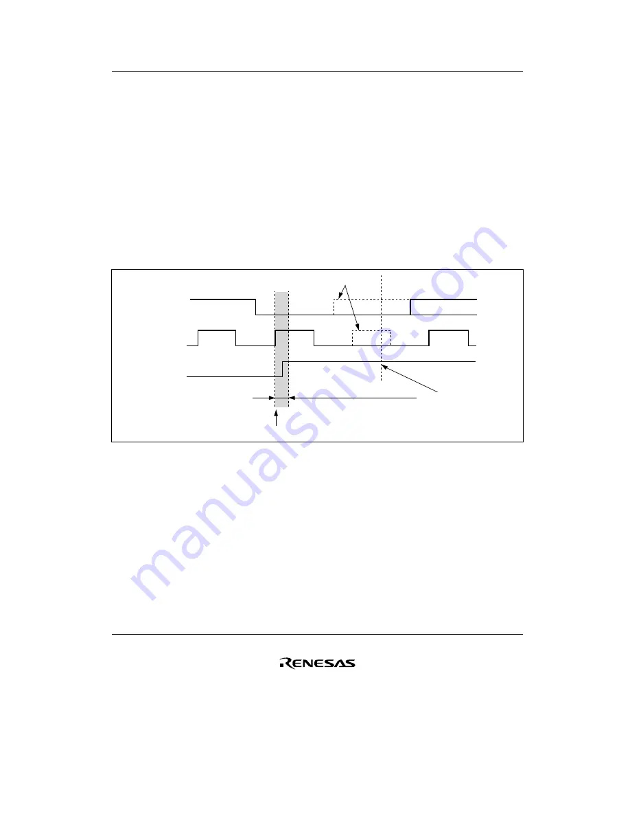
11. Note on ICDR read and ICCR access in slave transmit mode
In I
2
C bus interface slave transmit mode, do not read from ICDR or do not read from or write
to ICCR during the time shaded in figure 17.26.
However, such read and write operations cause no problem in interrupt handling processing
that is generated in synchronization with the rising edge of the 9th clock pulse because the
shaded time has passed before making the transition to interrupt handling.
To handle interrupts securely, be sure to keep either of the following conditions.
Read ICDR data that has been received so far or read from or write to ICCR before starting
the receive operation of the next slave address.
Monitor the BC2 to BC0 counter in ICMR; when the count is 000 (8th or 9th clock pulse),
wait for at least two transfer clock times in order to read from ICDR or read from or write
to ICCR during the time other than the shaded time.
Data transmission
Bit 7
Address reception
SCL
TRS bit
Waveform at problem occurrence
ICDR read and ICCR read/write are disabled
(Period of 6 system clocks)
8
R/W
A
9
The rise of the 9th clock is detected
SDA
ICDR write
Figure 17.26 ICDR Read and ICCR Access Timing in Slave Transmit Mode
12. Note on TRS bit setting in slave mode
In I
2
C bus interface slave mode, if the TRS bit value in ICCR is set after detecting the rising
edge of the 9th clock pulse or the stop condition before detecting the next rising edge on the
SCL pin (the time indicated as (a) in figure 17.27), the bit value becomes valid immediately
when it is set.
However, if the TRS bit is set during the other time (the time indicated as (b) in figure 17.27),
the bit value is suspended and remains invalid until the rising edge of the 9th clock pulse or the
stop condition is detected.
Therefore, when the address is received after the restart condition is input without the stop
condition, the effective TRS bit value remains 1 (transmit mode) internally and thus the
acknowledge bit is not transmitted after the address has been received at the 9th clock pulse.
Summary of Contents for H8S/2158
Page 10: ...Rev 3 00 Jan 25 2006 page viii of lii...
Page 36: ...Rev 3 00 Jan 25 2006 page xxxiv of lii B Product Lineup 863 C Package Dimensions 864 Index 865...
Page 47: ...Rev 3 00 Jan 25 2006 page xlv of lii Appendix Figure C 1 Package Dimensions TBP 112A 864...
Page 54: ...Rev 3 00 Jan 25 2006 page lii of lii...
Page 70: ...Section 1 Overview Rev 3 00 Jan 25 2006 page 16 of 872 REJ09B0286 0300...
Page 118: ...Section 3 MCU Operating Modes Rev 3 00 Jan 25 2006 page 64 of 872 REJ09B0286 0300...
Page 126: ...Section 4 Exception Handling Rev 3 00 Jan 25 2006 page 72 of 872 REJ09B0286 0300...
Page 198: ...Section 6 Bus Controller Rev 3 00 Jan 25 2006 page 144 of 872 REJ09B0286 0300...
Page 326: ...Section 10 8 Bit PWM Timer PWM Rev 3 00 Jan 25 2006 page 272 of 872 REJ09B0286 0300...
Page 440: ...Section 15 Watchdog Timer WDT Rev 3 00 Jan 25 2006 page 386 of 872 REJ09B0286 0300...
Page 606: ...Section 17 I 2 C Bus Interface IIC Rev 3 00 Jan 25 2006 page 552 of 872 REJ09B0286 0300...
Page 742: ...Section 19 Multimedia Card Interface MCIF Rev 3 00 Jan 25 2006 page 688 of 872 REJ09B0286 0300...
Page 750: ...Section 21 D A Converter Rev 3 00 Jan 25 2006 page 696 of 872 REJ09B0286 0300...
Page 768: ...Section 22 A D Converter Rev 3 00 Jan 25 2006 page 714 of 872 REJ09B0286 0300...
Page 770: ...Section 23 RAM Rev 3 00 Jan 25 2006 page 716 of 872 REJ09B0286 0300...
Page 824: ...Section 26 Clock Pulse Generator Rev 3 00 Jan 25 2006 page 770 of 872 REJ09B0286 0300...
Page 844: ...Section 27 Power Down Modes Rev 3 00 Jan 25 2006 page 790 of 872 REJ09B0286 0300...
Page 878: ...Section 28 List of Registers Rev 3 00 Jan 25 2006 page 824 of 872 REJ09B0286 0300...
Page 926: ...Index Rev 3 00 Jan 25 2006 page 872 of 872 REJ09B0286 0300...


