Chapter 18 NAND Flash Memory Controller
18-10
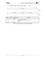
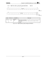
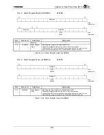
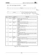
18.4.6 NAND Flash Memory Strobe Pulse Width Register (NDFSPR)
0xC014
31
16
Reserved
: Type
:
Initial
value
15
8
7 4
3 0
Reserved HOLD
SPW
R/W
R/W
:
Type
0000
0000
: Initial value
Bits Mnemonic Field
Name
Description
31:8
⎯
Reserved
⎯
7:4 HOLD
Hold
Time Hold Time (Initial value: 0000)
The output signals of the NAND flash controller (DATA[7:0], ND_CLE, ND_ALE and
ND_CE
*
) are held for HOLDxGBUSCLK cycles after the ND_WE
*
signal is
deasserted. When the NDFMCR.BSPRT bit is set to "1", the BUSSPRT
*
signal is
deasserted after this hold time is finished.
Note: This setting changes the read timing. The BUSSPRT
*
signal is deasserted
HOLDxGBUSCLK cycles after the ND_RE
*
signal is deasserted.
0000: 0
0001: 1xGBUSCLK
0010: 2xGBUSCLKs
0011: 3xGBUSCLKs
0100: 4xGBUSCLKs
0101: 5xGBUSCLKs
0110: 6xGBUSCLKs
0111: 7xGBUSCLKs
1000: 8xGBUSCLKs
1001: 9xGBUSCLKs
1010: 10xGBUSCLKs
1011: 11xGBUSCLKs
1100: 12xGBUSCLKs
1101: 13xGBUSCLKs
1110: 14xGBUSCLKs
1111: 15xGBUSCLKs
3:0 SPW
Strobe Pulse
Width
Strobe Pulse Width (Initial value: 0000, R/W)
These bits specify the Low pulse width of the ND_RE
*
and ND_WE
*
signals. The
low pulse width is the value of this field plus one.
0000: 1xGBUSCLK
0001: 2xGBUSCLKs
0010: 3xGBUSCLKs
0011: 4xGBUSCLKs
0100: 5xGBUSCLKs
0101: 6xGBUSCLKs
0110: 7xGBUSCLKs
0111: 8xGBUSCLKs
1000: 9xGBUSCLKs
1001: 10xGBUSCLKs
1010: 11xGBUSCLKs
1011: 12xGBUSCLKs
1100: 13xGBUSCLKs
1101: 14xGBUSCLKs
1110: 15xGBUSCLKs
1111: 16xGBUSCLKs
Figure 18.4.6 NAND Flash Memory Strobe Pulse Width Register (NDFSPR)
Summary of Contents for TMPR4925
Page 1: ...64 Bit TX System RISC TX49 Family TMPR4925 Rev 3 0 ...
Page 4: ......
Page 15: ...Handling Precautions ...
Page 16: ......
Page 18: ...1 Using Toshiba Semiconductors Safely 1 2 ...
Page 40: ...3 General Safety Precautions and Usage Considerations 3 18 ...
Page 42: ...4 Precautions and Usage Considerations 4 2 ...
Page 43: ...TMPR4925 ...
Page 44: ......
Page 54: ...Chapter 1 Features 1 8 ...
Page 58: ...Chapter 2 Block Diagram 2 4 ...
Page 88: ...Chapter 4 Address Mapping 4 12 ...
Page 226: ...Chapter 8 DMA Controller 8 58 ...
Page 260: ...Chapter 9 SDRAM Controller 9 34 ...
Page 480: ...Chapter 15 Interrupt Controller 15 32 ...
Page 554: ...Chapter 19 Real Time Clock RTC 19 8 ...
Page 555: ...Chapter 20 Removed 20 1 20 Removed ...
Page 556: ...Chapter 20 Removed 20 2 ...
Page 564: ...Chapter 21 Extended EJTAG Interface 21 8 ...
Page 580: ...Chapter 22 Electrical Characteristics 22 16 ...
Page 588: ...Chapter 24 Usage Notes 24 2 ...

