Chapter 16 CHI Module
16-2
16.2 Block
Diagram
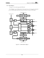
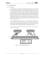
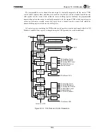
See Figure 16.2.1 for a block diagram of the CHI Module.
The CHI Module consists of holding registers (both transmit and receive), shift registers (both transmit
and receive), DMA support, and other logic to support interfacing to various types of TDM highways.
Figure 16.2.1 CHI Module Block Diagram
Control From CPU
MSB VS LSB First
Clock
and
Control
Logic
8B TX Shift REG
RX Hold Load
CHICLK
CHIFS
CHIDOUT
TXOE
Data from DMA or CPU
32B TX Hold REG-B
CHIDIN
Data to DMA or CPU
CLK
CMP
RX CH CNT
TX Shift Load
TX CH CNT
CHI
CTRL
and
STAT
REG
TX TDM
Switch
CTRL
REG
SYNCH
PRGM
Divider
OUT
REG
8
32
32
8
8
8
32B TX Hold REG-A
RX TDM
SWITCH
CTRL
REG
8B RX Shift REG
32B RX Hold REG-B
32B RX Hold REG-A
PRGM
Divider
SYNCH
SYNCH
CMP
MSB VS LSB First
Summary of Contents for TMPR4925
Page 1: ...64 Bit TX System RISC TX49 Family TMPR4925 Rev 3 0 ...
Page 4: ......
Page 15: ...Handling Precautions ...
Page 16: ......
Page 18: ...1 Using Toshiba Semiconductors Safely 1 2 ...
Page 40: ...3 General Safety Precautions and Usage Considerations 3 18 ...
Page 42: ...4 Precautions and Usage Considerations 4 2 ...
Page 43: ...TMPR4925 ...
Page 44: ......
Page 54: ...Chapter 1 Features 1 8 ...
Page 58: ...Chapter 2 Block Diagram 2 4 ...
Page 88: ...Chapter 4 Address Mapping 4 12 ...
Page 226: ...Chapter 8 DMA Controller 8 58 ...
Page 260: ...Chapter 9 SDRAM Controller 9 34 ...
Page 480: ...Chapter 15 Interrupt Controller 15 32 ...
Page 554: ...Chapter 19 Real Time Clock RTC 19 8 ...
Page 555: ...Chapter 20 Removed 20 1 20 Removed ...
Page 556: ...Chapter 20 Removed 20 2 ...
Page 564: ...Chapter 21 Extended EJTAG Interface 21 8 ...
Page 580: ...Chapter 22 Electrical Characteristics 22 16 ...
Page 588: ...Chapter 24 Usage Notes 24 2 ...


