Chapter 16 CHI Module
16-27
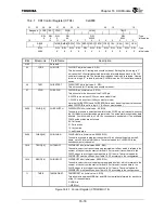
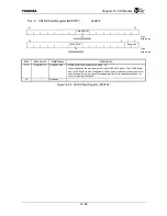
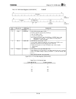
16.4.7 CHI SIZE Register (CHISIZE)
0xA818
31
30
29
18
17
16
Reserved DCNT
Reserved
R
:
Type
000000000000
: Initial value
15
14
13
2
1
0
B1TM DLOP
SIZE
RDEN TDEN
R/W R/W
W
R/W R/W
:
Type
0 0
000000000000
0 0
:
Initial
value
Bits Mnemonic Field
Name
Description
31:30
⎯
Reserved
⎯
29:18
DCNT[13:2]
CHIDMACNT
CHIDMACNT bits (Initial value: 0000_0000_0000, R)
These bits provide the status of the CHI DMA counter.
17:16
⎯
Reserved
⎯
15
B1TM
CHIBUF1TIME
CHIBUF1TIME bit (Initial value: 0, R/W)
The CHI DMA controller supports two buffer addressing modes depending on the
state of this bit.
0: the CHI DMA controller will loop back to the start of the DMA buffer when the end
of the DMA buffer is reached and will continue operating in a continuous and
circular manner.
1: the CHI DMA controller will stop executing when it reaches the end of the DMA
buffer.
14
DLOP
CHIDMALOOP
CHIDMALOOP bit (Initial value: 0, R/W)
This bit selects loopback modes depending on the state of this bit.
0: not loopback mode.
1: loopback mode(This ordering allows an RX-to-TX immediate loopback via the
DMA buffer. Please refer to the chapter of 16.3.4
13:2
SIZE[13:2]
CHISIZE
CHISIZE bits (Initial value: 0000_0000_0000, W)
These bits define the size of the CHI DMA buffers (16 bytes minimum/16 Kbytes
maximum). Both the CHI RX buffer and the CHI TX buffer are the same size. The
last address in the CHI RX DMA buffer is given by CHIRXSTART[31:2] ·
CHISIZE[13:2]. The last address in the CHI TX DMA buffer is given by
CHITXSTART[31:2] · CHISIZE[13:2]. The value loaded into CHISIZE should be
equal to the desired buffer length-1.
1
RDEN
CHIRXDMAEN
CHIRXDMAEN bit (Initial value: 0, R/W)
This bit enables the CHI DMA receive function.
This bit should not be set until the CHIRXSTART, CHITXSTART, and CHISIZE
registers are setup. To enable CHI DMA receive function, this bit must be set before
the CHI Module is enabled (ENCHI asserted). Either CHIRXDMAEN or
CHITXDMAEN or both can be set at a time since the CHI DMA controller can
support full duplex operation.
0: Disable
1: Enable
0
TDEN
CHITXDMAEN
CHITXDMAEN bit (Initial value: 0, R/W)
This bit enables the CHI DMA transmit function.
This bit should not be set until the CHIRXSTART, CHITXSTART, and CHISIZE
registers are setup. To enable CHI DMA transmit function, this bit must be set
before the CHI Module is enabled (ENCHI asserted). Either CHIRXDMAEN or
CHITXDMAEN or both can be set at a time since the CHI DMA controller can
support full duplex operation.
0: Disable
1: Enable
Figure 16.4.7 CHI SIZE Register (CHISIZE)
Summary of Contents for TMPR4925
Page 1: ...64 Bit TX System RISC TX49 Family TMPR4925 Rev 3 0 ...
Page 4: ......
Page 15: ...Handling Precautions ...
Page 16: ......
Page 18: ...1 Using Toshiba Semiconductors Safely 1 2 ...
Page 40: ...3 General Safety Precautions and Usage Considerations 3 18 ...
Page 42: ...4 Precautions and Usage Considerations 4 2 ...
Page 43: ...TMPR4925 ...
Page 44: ......
Page 54: ...Chapter 1 Features 1 8 ...
Page 58: ...Chapter 2 Block Diagram 2 4 ...
Page 88: ...Chapter 4 Address Mapping 4 12 ...
Page 226: ...Chapter 8 DMA Controller 8 58 ...
Page 260: ...Chapter 9 SDRAM Controller 9 34 ...
Page 480: ...Chapter 15 Interrupt Controller 15 32 ...
Page 554: ...Chapter 19 Real Time Clock RTC 19 8 ...
Page 555: ...Chapter 20 Removed 20 1 20 Removed ...
Page 556: ...Chapter 20 Removed 20 2 ...
Page 564: ...Chapter 21 Extended EJTAG Interface 21 8 ...
Page 580: ...Chapter 22 Electrical Characteristics 22 16 ...
Page 588: ...Chapter 24 Usage Notes 24 2 ...

